
Before going into the details, I’ll talk about how the high level design has evolved:
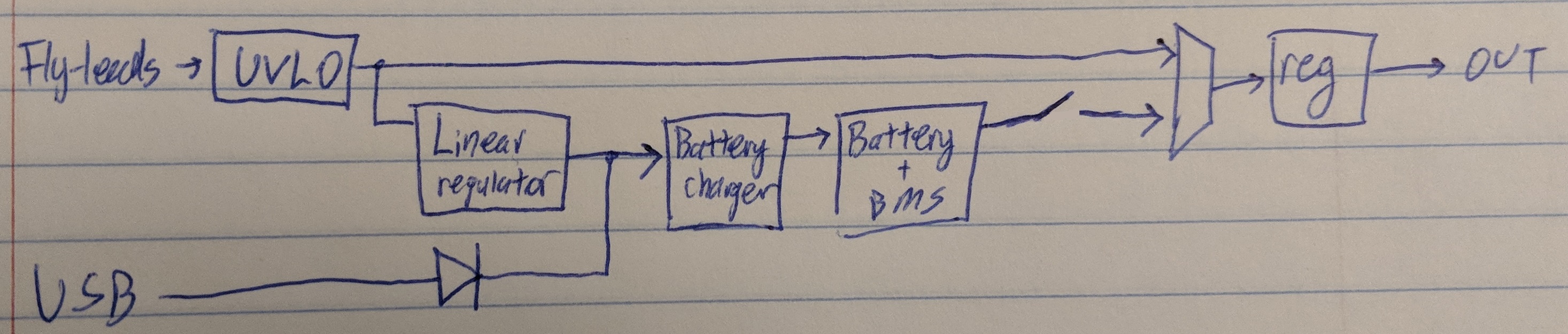
- There are 3 potential sources of power: the fly-leads, the USB and the battery. I’ve decided that the USB should only charge the battery, and not power the output regulator directly. This was done to 1) reduce the complexity of the power multiplexing and 2) limit the current draw through the USB. Limiting the current draw on the USB is very important as trying to draw too much may damage the USB port on the power source side; for example, if it’s plugged into a laptop, the laptop may be damaged. Conveniently, the battery charging circuit will have a current limit to protect the battery; in this case, it will double to protect the USB as well.
- The fly-leads are assumed to be capable of outputting a large amount of current over a wide range of voltages; say up to 12 volts. Because of this, the fly-leads will be given priority over USB when it comes to charging the battery, and it will be chosen over battery when it comes to powering the output regulator. This way, you can provide power through fly-leads and not load the USB port or the battery.
- There will be 2 power multiplexers. The first will choose between the fly-lead power source and USB for charging the battery; this will be done by comparing the two sources and going with the one with higher voltage, accomplished using a diode. The second will be choosing the battery voltage or the fly-lead to power the output regulator. This will be done by checking if the fly-lead power is present, and choosing that if possible. In both cases, if the fly-lead power is close in voltage to the USB voltage or the battery voltage, the multiplexer may become confused or current may flow in the wrong direction. To prevent this, the fly-lead power source will have an UVLO (under-voltage lockout) circuit, which will prevent the fly-lead power source from providing any power until the voltage exceeds a certain amount.
- The wide voltage range that the fly-leads could be presents a problem for the battery-charging circuit for two reasons. One, the battery charging IC can only accept voltages up to 6 volts. Two, even if it could accept 12 volts, it would output at worst case around 3 volts. This means that it would have 9 volts across it, and since most battery charging ICs are linear (as opposed to switching), this will mean the chip will have to withstand a large amount of heat dissipation. This concern was addressed by putting a linear regulator on the input of the battery charging circuit.
- I’ve added a switch to disconnect the battery from the circuit. When not in use, the circuit’s power consumption is low, and the BMS (battery management system) IC should prevent the battery form being drained too much. However, for long term storage (or to make sure the battery is not loaded), the switch will completely disconnect the battery from the circuit, preserving energy.
- The circuit is designed to use a lithium-ion / lithium-polymer battery that can tolerate a voltage of 2.75 volts to 4.232 volts. The maximum charge and discharge rates can be adjusted, but for now are set to around 100 mA.
The updated functional block diagram looks like this:
Here’s a breakdown of the schematic:
Fly-lead input + UVLO
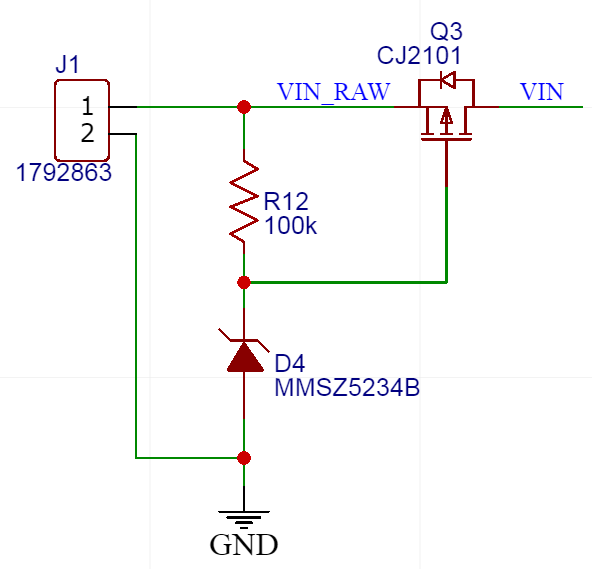
The fly-leads will come onto the board on J1. I wanted the project to be as user-friendly as possible, so J1 was selected to be a connector that didn’t require tools to insert and remove wires.
The UVLO circuit works by using 2 components: a PMOS and a zener diode.
- A zener diode is like a regular diode except it has a very low breakdown voltage. This means that the zener diode will not conduct current until the voltage across it exceeds a certain amount (around 7 volts in this case); then, the diode will try to resist a further increase in voltage by conducting current. The diode can begin to conduct a very large amount of current, so it is current limited by the 100k resistor.
- The PMOS will not conduct current until the gate is certain number of volts below the source. The source connects to VIN_RAW, while the gate connects to the cathode of the zener diode.
The circuit operates as follows: when the input voltage is below 7 volts, the zener diode does not conduct current. Thus, because there is no current drop across the 100k resistor, the source and the gate of the PMOS are the same, meaning the transistor does not conduct. When the input voltage exceeds 7 volts, the diode will conduct, forcing the gate to remain around 7 volts, while the source will exceed 7 volts. Since the source now has a higher voltage than the gate, the PMOS will conduct, allowing the rest of the circuit to be powered by the fly-leads.
The PMOS allows the power source to be disconnected from the circuit by cutting off the high voltage. However, another way to kill power is disconnecting the ground connection. Disconnecting the ground is preferred in most cases, as to disconnect the ground, an NMOS is used, which is more power efficient than a PMOS. However, I opted to use a PMOS in case the USB and the fly-leads shared the same ground. If they did in fact share the same ground, and an NMOS was used, than the UVLO circuit would not work.
Linear Regulator and USB
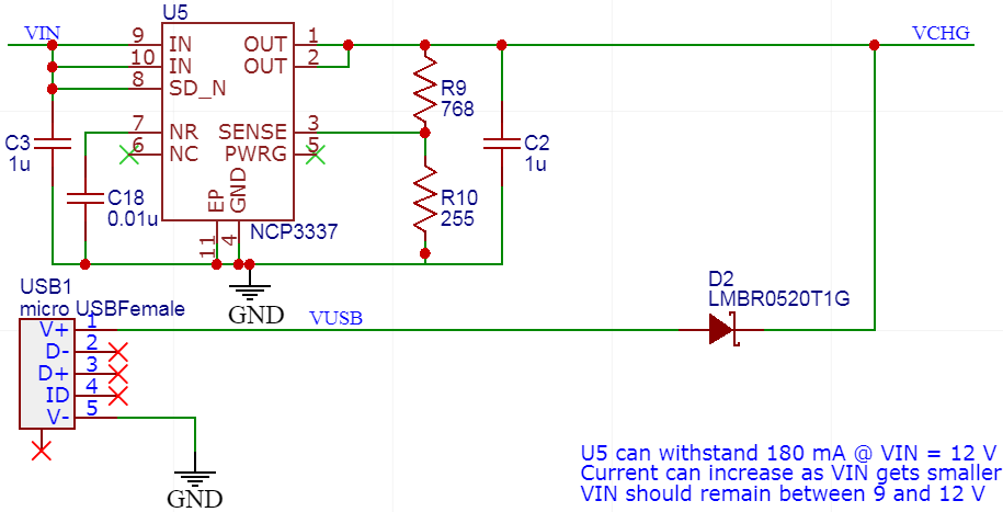
The fly-lead power supply then goes into a linear regulator, reducing the voltage to 5 volts. I initially wanted to use a regular linear regulator; however, the drop-out voltage requirements (which sets the minimum usable input voltage), made using a regular linear regulator an unattractive option as it would reduce the functional voltage range for the fly-leads. I therefore decided to use an LDO (low drop-out) regulator. I was wary of these devices because their stability often depends on the ESR (equivalent series resistance) of the output capacitor, which sounds very shady to me. That’s right: if you use a ceramic capacitor (which has minuscule ESR in most cases), the regulator will not work! However, I found the NCP3337, which has many attractive features like being stable with any type of output capacitor, no need for external compensation, simple input and output bypass capacitor requirements, and reverse current protection. The last feature is very useful in this case, and is the reason why the output of the regulator doesn’t require a diode to protect the power supply connected to the fly-leads.
The USB connection is very simple. The connector will provide a connection to a micro-USB cable, and the diode will prevent the linear regulator from driving current out onto the cable. The diode is a low power Schottky diode, which has a relatively low forward voltage drop. The low forward voltage drop will improve power efficiency of the system.
Battery Charger
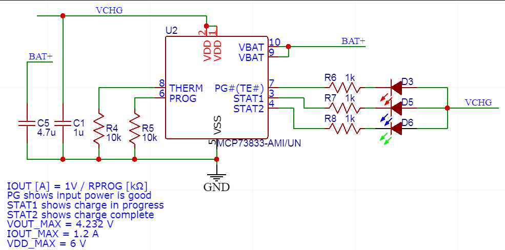
The battery charging circuit has the MCP73833 at its heart. The battery charger will output a constant current when the battery is not almost full. This current value can be set by changing the resistor value connected to the PROG pin (10k in this case, setting the current to 100 mA). When the battery is almost full, the charger will change to a constant voltage mode, which will cause the battery to charge more slowly. What the output voltage is depends on the chip’s part number. For this design, we assume the battery should not be charged above ~4.2 volts, so I got the chip that will only output a maximum voltage of 4.232 volts. The LEDs will show the status of the input voltage and the battery charging, which is very useful, but can be removed if not needed. Lastly, a thermistor can be used in this circuit, but is not used in this application.
BMS
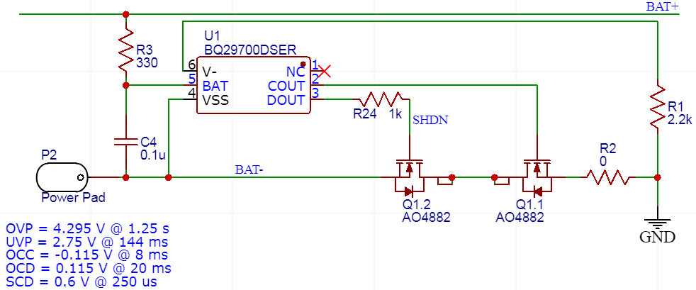
BQ297000DSER is the BMS IC. It will disconnect the battery from the rest of the circuit if it detects that the battery voltage becomes too high or too low, or it detects the input or output current is too high. This will extend the life of the lithium-ion / lithium-polymer battery, but more importantly it will prevent the battery from exploding or catching fire. The IC monitors the overvoltage, undervoltage, overcurrent charge and overcurrent discharge conditions by monitoring the voltage on its V- pin and BAT pin.
The BAT pin sensing is pretty self-explanatory: if the battery voltage becomes too high, prevent charging; if the battery voltage becomes too low, then prevent discharging. Both of these actions are done by turning off either Q1.1 or Q1.2. V- sensing, on the other hand, I wasn’t as sure about; it’s attempting to measure current by measuring a voltage at one point. I suspect that the chip relies on the on-resistance of the NMOS transistors (Q1.1 and Q1.2) to generate a voltage that is proportional (or close to proportional) to the battery’s output current. However, the on-resistance of the transistors is not a closely controlled value, and varies with the chip itself, time, temperature, etc. In addition, if you want to set a specific current limit, you would have to pick specific transistors that have a very specific on resistance. In order to ease this limitation, I put R2 in series with the transistors so that the on-resistance could be artificially increased, allowing the user to adjust the current limit by changing the value of the resistor. I also put a resistor in between the gate of Q1.2 and the output of the IC to prevent output contention, which I’ll talk about more in the next section.
As a minor note, I really don’t like this chips footprint because it it tiny and leadless, making it very difficult to solder. It also tolerates too much overvoltage for my liking. However, it was the best one I could find that was available and close to what I needed. The overvoltage shouldn’t be a problem as long as the battery is charged using the charging circuit discussed earlier.
Battery Switch
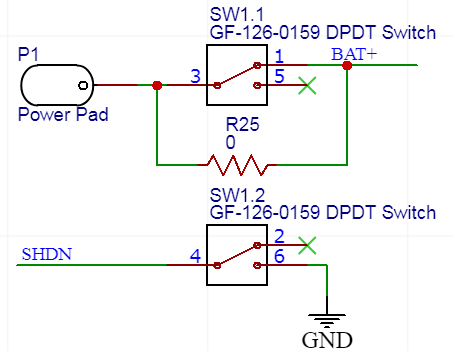
To quickly disconnect the battery for storage or to turn off the circuit, a switch was added to disconnect the battery from the circuit. SW1.1 will have current going right through it, so flipping this switch will disconnect the battery. The switch is rated for 500 mA, which is more than enough for this application. However, in case some want to have more than 500 mA, a 0 ohm bypass resistor can be added, saving the switch. But if you add that, how do you prevent the battery from discharging? That’s where SW1.2 comes in. During regular operation, SHDN is driven by the BMS IC, allowing it to turn on and off the discharge transistor as it sees fit. However, if SW1.2 is changed to the other position, SHDN becomes grounded, forcing the discharge transistor to turn off, electrically disconnecting the battery from the circuit. The 1 kohm resistor on the output of the BMS IC prevents the switch from shorting the output to ground.
Power Multiplexer
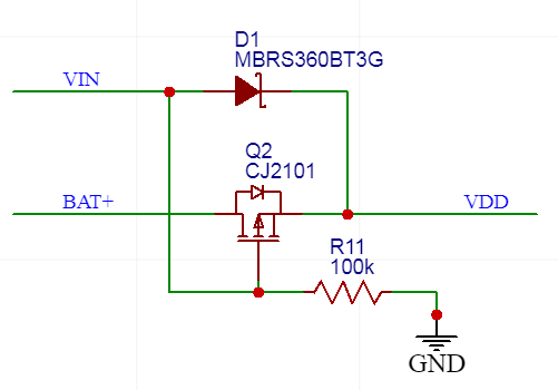
The power multiplexer chooses what will power the output regulator: the fly-lead power supply, or the battery. It does this by using a PMOS, and is somewhat similar to the UVLO circuit described earlier. If no voltage is supplied through the fly-lead connector, than the gate of Q2 will be near 0 volts, while the source will be close to the battery voltage. This will turn the PMOS on, and the battery can provide power to the output regulator. If voltage is non-zero at VIN (and thanks to the UVLO we know that the voltage will be 7 volts or greater in this case), than the gate voltage will be higher than the battery voltage (which goes up to 4.2 volts at most), so the transistor will remain off. This will prevent the battery from powering the output regulator. The transistor is the main reason the UVLO is necessary; if there was no UVLO, and VIN was about the same voltage as BAT+, than the transistor will be partially conductive, which will allow an unrestricted amount of current to flow from VIN to BAT+, which may damage the battery. The BMS should protect the battery at worst case, but I wanted to add an extra layer of security. The Schottky diode D1 prevents current from flowing out of the battery and going out through the fly-leads.
Buck-Boost Regulator
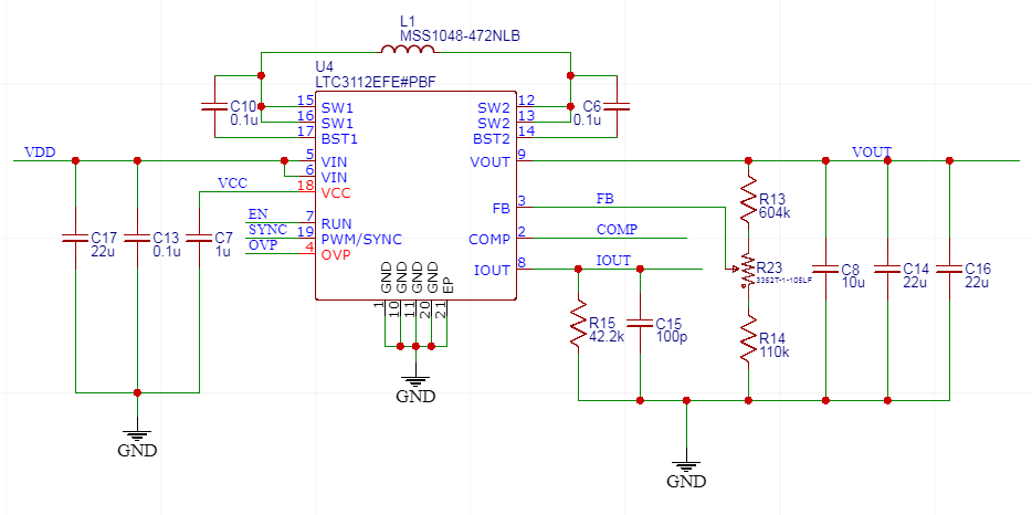
I chose the LTC3112 buck-boost regulator for several reasons, despite its high cost:
- It has a very wide input and output voltage range
- It has high output current capabilities
- It has a model in LTSPICE, allowing the design to be tested
The circuit shown above is mostly similar to the one given in the datasheet. The only comment I have to make here is the feedback pin; I used a potentiometer to make the output voltage adjustable. R23 is a 1 megaohm potentiometer, and R13 and R14 are used to set the minimum and maximum output voltage of the regulator, which are (in theory) 1.24 volts and 12.47 volts. Another reason these particular values were chosen was due to the regulator’s requirement that the output impedance of the feedback path to the feedback pin must be greater than 100 kohms, which this design accomplishes.
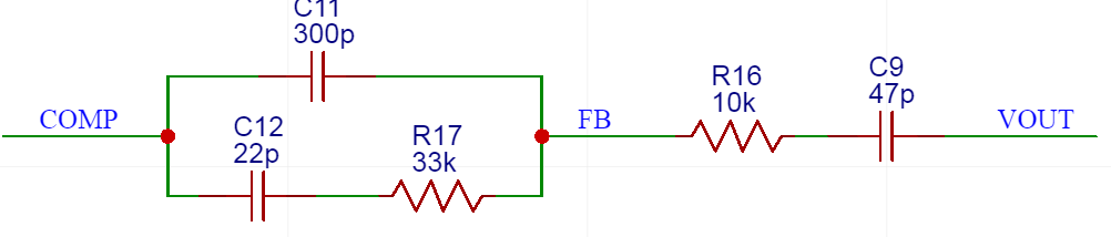
I wish I could comment on the compensation network, which will define how the regulator reacts to transients and during start-up. However, this is a subject I don’t understand very well myself; I’m hoping to have a post about it at a later time exploring this subject. For now, I kept tweeking the values in LTSPICE and running simulations until I got a start-up behavior I liked. I’ll need to do testing after the circuit is built to verify the results, but for now I’ll use these values.
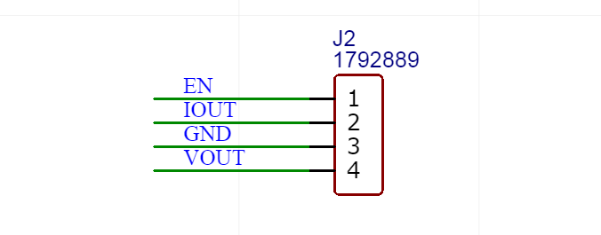
This is the same type of connector as the input connector for the fly-lead: no tools required. I also wanted to have more available on the connector than just ground and power output to make the design more flexible and user-friendly. I therefore added an enable pin, in case an external circuit wants to control the regulator, and IOUT, which indicates how much average current the regulator is outputting.
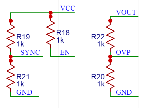
The resistor shown here set how the regulator behaves. SYNC can be tied high or low to make the regulator operate in PWM or Burst Mode respectively (latter is better suited for low power applications than the latter). OVP can be used to set over-voltage protection, preventing the regulator from outputting if the input voltage is too high. SYNC will be set to PWM, and OVP will not be used.
Conclusion
This concludes the overview of the schematic. We have discussed how the fly-lead power supply input will be conditioned, how the battery will be charged, how the battery will be ensured to operate safely, how the output regulator will be powered, and how it has been designed. Next, we’ll move on to the layout, where I do an overview of the layout.
