The thermal regulator is responsible for two things:
Reporting the temperature of the load
Controlling the fan speed for cooling the load
The thermal regulator accomplishes the first objective by measuring the output of the thermal regulator circuit with the ATMEGA32U4’s ADC. The second objective is accomplished by converting the load’s temperature to a duty cycle. Let’s take a look at the hardware and software of getting the temperature.
Thermistor OPAMP circuit
The thermistor circuit is shown above; the thermistor is in parallel to C39 and R24. This circuit converts the resistance of the thermistor, which depends on temperature, to a voltage that can be read by the ADC.
Voltage as a function of temperature
The graph shows TOUT as a function of temperature. Unfortunately, the output is not linear, so this conversion must be reversed in the software; that is, the temperature must be calculated from TOUT.
Temperature as function of voltage
The image above shows deriving the equation for converting voltage to temperature. On the left is the table of temperature and voltage. In the middle is the graphs showing the data, and below that is 1st, 2nd and 3rd order equations for calculating the temperature as a function of voltage. On the right shows the calculated temperatures using the temperature equations, and the errors for each temperature.
Macro for voltage-to-temperature conversion
The macros above shows how to convert the voltage to temperature. The first, second and third order equations are defined, and then SCH_TR_VOLT_TO_TEMP chooses which order to use. In this case, the second order equation is used.
Now let’s look at how the temperature is used to calculate duty cycle:
Converting temperature to duty cycle
In the software, Tmin, Tmax, Dmin and Dmax are defined in macros. For example, the minimum allowed duty cycle will be Dmin, which corresponds to Tmin, and the same for Dmax and Tmax. The equation above shows calculating the duty cycle when the temperature falls between Tmin and Tmax. It should be noted that if t is below Tmin, then the calculated duty cycle will be below Dmin, and if t is above Tmax, then the calculated duty cycle will be above Dmax. However, this is irrelevant in this case since Dmin and Dmax are 0 and 100 respectively, and the PWM code will interpret negative numbers as 0 and values above 100 as 100. Currently, Tmin is set to 35 °C, and Tmax is set to 85 °C. It should also be noted that though the equation above shows the equation using temperature, in the code the duty cycle is calculated using voltages. This is because I coded the voltage-to-duty-cycle code before I calculated the voltage-to-temperature equation. I should update that in the future.
Now that we know how to calculate temperature and duty cycle, let’s look at the code:
Temperature Regulator constructor
The constructor for the temperature regulator is very simple. First, last_time is zeroed, which is used to see if enough time has passed to run the regulation code. Second, enable is set to true. If the temperature regulator is enabled, then duty cycle depends on the measured temperature. If temperature regulator is disabled, then duty cycle will stop changing based on the measured temperature, allowing the user to manually set the fan speed. Third, the target duty cycle is initialized to zero.
Regulate method
Above is the code used to regulate the fan temperature. First, the method sees if enough time has passed to run this code. If it has, then the ADC is read and the result is saved in volts. Then, temperature is calculated using the 2nd order equation, with temp_volt as the argument. Next, enable is checked. If enable is true, then the duty cycle should be calculated using temperature, or temp_volt in this case. If enable is false, then duty cycle is set to target_duty_cycle. target_duty_cycle is initialized to zero, but it can be changed through the user interface.
Note: the control loop, discussed later, has been updated. See System Testing.
Let’s take a look at the heart of the variable load project: the code to regulate the load.
Architecture of the load regulator
The load regulator module has four major components:
LTC2451: This is the current monitor. This ADC is connected to the output of the hall-effect sensor, and communicates with the microcontroller through the I2C / TWI bus.
MAX5216: This is the DAC the microcontroller uses to affect the amount of current flowing through the load. 0 amps corresponds to a DAC output of 0.5 V, and each 80 mV on top of that allows an additional amp to flow through the load.
AD8685: This is the ADC used to measure the voltage across the load. The input voltage is put through a voltage divider, which is then read by this ADC. The software accounts for the scaling-down of the input voltage and then scales it back up.
Timer 1: This is the timer the load regulator uses for timing its actions. For example, the current through the load is measured 60 times per second, or every 17 ms. The load regulator will check its timer to see if 17 ms have passed.
LoadRegulator members
Above, the image shows the LoadRegulator class’ members. The HAL class members are members necessary for the device classes to work. current_monitor, which is an instance of the LTC2451 member, uses HAL_TWI. current_control, which is an instance of MAX5216, uses a GPIO class for its chip select, and SPI class for communication. volt_monitor, an instance of ADS8685, also uses GPIO and SPI. The data members are variables the LoadRegulator classes uses for its operations.
cal_zero: In theory, at zero current, the hall effect sensor should output 0.5 volts. However, it’s extremely unlikely the output will be exactly 0.5 volts. Therefore, it’s best to figure out what the actual output voltage at zero current is. This voltage is stored here.
target_current, target_power, target_resistance, target_voltage: the load regulator will need to know what target to aim for. In constant current mode, the amount of current flowing through the load should be target_current. Likewise, in constant power mode, the amount of power the load dissipates should be target_power. Same goes for target_resistance and target_voltage.
measured_current: every time the current through the load is measured, the value is stored here.
control_current: this is the knob the module will turn to adjust the current through the load. If measured_current is too small, then control_current is increased. If measured_current is too large, then control_current is decreased.
measured_voltage: every time the voltage across the load is measured, the value is stored here.
There are two miscellaneous members. First is last_cur_time. This variable stores the last time the current sensor was read. Second is op_mode. This determines what mode the load regulator is in: off, constant current, constant power, constant resistance, or constant voltage.
LoadRegulator constructor
Above is the constructor. The initialization list is pretty long since this class has so many class members. But thankfully, whatever calls this constructor doesn’t have to worry about providing it with arguments, making this class easy to create. The reason no arguments are necessary is because of the project header files, schematic.h and settings.h. Everything with a SET prefix comes from settings.h, while everything with a SCH prefix comes from schematic.h. Since all the information like timer settings and GPIO pin, port and direction are stored in these header files, the initialization list can use that information and set up all the class members without depending on arguments.
Let’s look inside the constructor. First, the timer that was set up in the initialization list (LR_Timer) has its interrupt enabled. This is necessary for the timer to work, since the timer’s interrupt increments a counter that allows us to measure the passage of time. Then, the voltage monitor is configured. The voltage monitor ADC, ADS8685, has a lot of settings that can be adjusted. The two of interest here are the programmable gain amplifier, which determines the input range, and the reference voltage, which affects the ADC’s resolution. After that, target_power, target_resistance and target_voltage are set to default values. Lastly, some house keeping is done to prevent damaging the load or external power supply on power up.
Regulate method
This is the method that actually regulates the load, and it is called in the main loop. LR_Timer is configured to set a flag every 1 ms, so the code will run at that frequency. Firstly, after clearing the flag, the system sees if it should sample the current monitor. The current monitor ADC has a sample rate of 60 Hz, so there’s no point sampling faster than that, and unnecessary and futile attempts to communicate with the ADC takes up bandwidth on the I2C bus. If the measurement is successful, then measured_current is updated, and error is updated to reflect that the read was successful. Then, the voltage across the load is measured, and measured_voltage is updated. Measuring current and voltage is done in preparation for the next step: the regulation of the load. The load regulator operates at 60 Hz for CC, CP, and CR mode. This is because CC, CP and CR regulation can only run when the current is successfully measured. However, CV only needs a successful voltage reading to run, so it can run at the 1 kHz rate. If the regulator is in the OFF mode, then the current through the load is set to 0.
Adjust Control Current method
The code above shows the method used to adjust the control current. Say the user requests a current through the load of 1 A, and the current monitor reports a current reading of 0.5 A. Clearly, the current needs to be increased by 0.5 A. If the user requests 1 W from a 5 V power supply, and the system is only consuming 0.1 A (or 0.5 W), then the current has to be increased by 0.5 W / 5 V = 0.1 A. Likewise, if the resistance is too small or large, then current through the load is adjusted to approach the desired resistance value.
Instead of adding the error to control_current, I use SET_LR_CUR_ERROR_SCALER to adjust how quickly the system approaches the requested value. Currently, it’s set to 1/2. This means that if an error is 0.5 A, then the output is changed by half that, so 0.25 A. This dampens the systems response so that there are no overshoots. I’ll play with this value in the future to see if it’s necessary, but for now 0.5 is a decent place holder.
CC, CP and CR control loop Software compares target value to measured value, then adjusts accordingly
Above shows the control loop. As mentioned, the target value and measured voltage are used to calculate the required current through the load, and then the software will compare the required current with the measured current. Since measured current is limited to the sample rate of the ADC, which is 60 Hz, this loop can only run at 60 Hz at most. This is a shame since measured_voltage updates at 1 kHz, but that will not help the loop run faster. It will, however, help the load regulator in CV mode.
CC, CP and CR are all very similar since it is possible to calculate how much current is necessary based on the desired target current, power or resistance and the voltage across the load. For example, if the user requests power P, and the voltage across the load is V, then the current through the load should be P/V. If the user requests resistance R, and the voltage across the load is V, then the current through the load should be V/R. However, this is not possible for CV; if the user requests voltage V across the load, then how much current should flow through the load? The answer is unknown, so the code has to guess. Unlike CC, CP and CR which can calculate the necessary output and approach it, CV just measures the voltage across the load and increases the current if the voltage is too high, or decreases it if the voltage is too low. The step size is set by SET_LR_CV_CUR_STEP, which is currently set to 1 mA. Since CV runs 1000 times per second, that means the current through the load can change 1 A per second. Hopefully that’s good enough, but I will add the disclaimer that CV isn’t the system’s strong suit. Also, putting the load regulator on the output of a constant voltage power supply with no current limiting resistor can cause the power supply to become unstable, since the power supply and variable load will be fighting for dominance.
Calibrate Zero method
Part of the house keeping in the constructor is calibrating the zero. In the system, ideally the output of the hall effect sensor, and therefore the input to the ADC, is 0.5 V at no current flow. However, this cannot be assumed. Therefore, the ADC input at zero current must be found, and this value is stored in cal_zero. The code above shows how this is done: assuming the load has no current flowing through it, the current monitor is read SET_LR_CAL_AMOUNT times, which is currently 10. Then, cal_zero stores the average of those 10 readings.
I hope you enjoyed reading about the load regulator section of the code. Next, let’s take a look at the thermal regulator.
Normally, the software architecture would be defined at the start of the project, or before programming begins. However, I didn’t really know how I wanted the code to look back then, so I decided to work on the hardware abstraction layer. Now, most of the low level drivers are complete. Therefore, it seems like the right time to talk about the software at a high level.
Overview
System Architecture Blocks rely on the blocks below it (eg. LCD uses TWI)
Here’s an overview of the code. The code will consist of 4 modules: the temperature regulator, which keeps the load from getting too hot, the load regulator, which controls the current through the load, the user interface, which allows the user to interface with the system, and the debugger, which is used to get information about the system. I’ll elaborate on each module below, as well as in future posts.
Main is the glue that holds the system together. Firstly, it hosts an instance of each module, and calls methods from the modules. Secondly, it allows modules to share information. Lastly, it has the main timer, which is Timer 3. This is the clock referenced by most modules for time keeping. In this application, Timer 3 will increment a counter every millisecond. The modules that use the timer will use this counter to know how much time has passed. For example, if the temperature regulator runs every 100 ms, then the module will keep checking the counter and do nothing until the counter has increased by at least 100 since the last time the module was run. This way, one timer can be used to coordinate the activities of multiple modules.
Schematic.h contains information dependent on hardware; most of this information comes from the schematic and datasheets for the chips in the schematic. Examples of information contained here are:
What SPI mode devices on the SPI bus operate in
Clock speeds for different SPI and I2C devices
What the reference voltage is for different devices
Equations to convert counts to voltages for ADCs
GPIO’s port, pin and direction
If an LED is active high or active low
Settings.h contains information that doesn’t derive from hardware. Examples of information contained here are:
Configuration settings for Timer 1 and Timer 3
How frequently different modules are run
UART format (eg. 8N1)
How data is displayed on the LCD (eg. how many decimal points)
Both header files are used by main as well as the modules. This way, when a module is being constructed, main doesn’t have to provide low level information like what port and pin a GPIO should be on; the module can do that by itself by reading the Schematic.h header file. This keeps high level code clean, and the relevant information consolidated into few files.
Temperature Regulator
The temperature regulator is probably the simplest module. Its job is to keep the variable load, the transistor, from getting too hot. This means the temperature regulator must (a) know the transistor’s temperature, and (b) take action to adjust it.
The hardware allows for both of this. Firstly, the transistor will have a thermistor attached to it, and an opamp on the circuit board converts the thermistor’s resistance to a voltage. This voltage is then fed into ATMEGA32U4’s ADC. This allows the temperature regulator to determine the transistor’s temperature by reading from the ADC. Secondly, the variable load is hooked up to a head sink with a fan on it. How hard the fan blows can be controlled by a PWM signal, which is hooked up to the microcontroller. If the temperature regulator sees that the ADC count it too high, which indicates that the transistor is getting too hot, then the PWM’s duty cycle is increased. If the transistor cools off and the ADC count drops down, then the PWM’s duty cycle can be decreased to reduce fan noise.
The temperature regulator doesn’t need to be run very often, since the large heat sink the transistor is mounted on will prevent rapid changes in temperature. For now, the temperature regulator will run every 100 ms, at which point it samples the ADC and determines what the PWM’s duty cycle should be.
Load Regulator
The load regulator is the heart of the project. It is responsible for controlling the current going through the transistor. LTC2451 is the current monitor, and it is used to determine how much current is going through the load. MAX5216 is the DAC that allows the microcontroller to control how conductive the transistor is. ADS8685 is the ADC that tells the microcontroller how much voltage is across the load.
In constant current mode, the load regulator will be told to allow a certain amount of current through the load; say 1 amp. In this scenario, the load regulator will read LTC2451 to see how much current is going through the load. If it’s below 1 amp, then MAX5216 is updated to allow more current. If it’s above 1 amp, then MAX5216 is updated to reduce the current flow. In constant power and constant resistance mode, the load regulator is told to make the load dissipate a certain amount of power, or to have a certain amount of resistance. The load regulator will use this information, and the amount of voltage across the load (information provided by ADS8685) to calculate how much current should flow through the load. Then, like in constant current mode, the load regulator uses LTC2451 and MAX5216 to try to achieve that current.
Constant voltage mode is a unique case. Here, the load regulator doesn’t care how much current flows through the load. It only cares about the voltage across it. Therefore, it will read ADS8685 to see how much voltage is across the load, and then update MAX5216 accordingly. If the voltage is too high, then increase current consumption; if voltage is too low, decrease current consumption.
How frequently the load regulator is run depends on the mode of operation. For constant current, power and resistance mode, the control loop needs to know how much current is flowing through the load, so LTC2451 must be read constantly. Since LTC2451 can only sample at 60 Hz, the control loop only runs 60 times per second, which is around every 17 ms. Meanwhile, in constant voltage mode, LTC2451 isn’t used in the control loop, so the control loop can be run at a higher frequency. I’ll use 1 kHz, or every 1 ms, for now, and see how that goes.
User Interface
The user interface has two jobs. Firstly, it must display information to an LCD screen. This display will show things like the voltage across the load or the amount of current flowing through it, but the display will also be used to navigate menus and settings. Secondly, the user interface will handle input from the user via an encoder. The encoder can turn clockwise or counter-clockwise, and it can also be pressed like a button. These actions will allow the user to change screens, navigate the menu, and change the system’s behavior.
The LCD library, which uses the TWI HAL, will allow the module to write characters to the display. The encoder library, which uses the GPIO HAL, will read user input. The Screens library will tell the user interface module what to do with the input from the encoder, as well as what text should be displayed on the LCD. The user interface is responsible for forwarding the encoder input to the Screens instance, and then outputting information to the LCD, as instructed by the Screens instance.
Updating the LCD display too frequently will make it hard to read, just like how rapidly flipping through the pages of a book makes it illegible. Therefore, I’ll have the display update once every second. However, if I’m navigating through a menu, then waiting a whole second every time I want to move the onscreen cursor would be maddening. Therefore, the display will update every second, or whenever the user provides an input through the encoder.
Debugger
The debugger allows the system to communicate with a computer through a serial, or COM, port. I’m currently using it to interface with the system before I have the user interface module up and running, since that’s my only other way of getting information into or out of the system. I’m not 100% sure yet what the debugger will be used for once the user interface is complete, but I’ll figure that out later. It might not be a bad idea to have the user interface module and the debugger fill the same role; that way, I can control the load via encoder, or through a terminal.
The debugger creates strings that contain information like the amount of voltage across the load or the amount of current flowing through it. It then sends this information out over UART. The UART can also receive information from the serial port, which is stored in a ring buffer. The debugger also has LEDs it can use to quickly indicate when an event has occurred. I currently only use one LED; it is on when the load regulator is running, and off otherwise. I’m using it to see how long it takes for the load regulator to run, and to confirm it is running at the right frequency; however, as more of the code gets written, I’m sure more LEDs will be used up.
The debugger has a lot of strings and performs a lot of string manipulation; this means the debugger is very memory and CPU intensive. This may necessitate removing the debugger if I run out of memory, or it adversely affects system performance. We’ll have to see as more of the code gets fleshed out.
The debugger is run once a second; at this point, it prints a message to the console on the computer, showing useful infomration. The debugger also checks if input was received from the console, and acts accordingly on that input. The input is used to change the load regulator’s mode of operation (constant current, power, etc.) as well as the target value (1 A, 5 Ω, etc.).
Conclusion
I hope you enjoyed the quick overview of the system architecture. Next, we’ll walk through each module and get a deeper understanding of they work.
I2C, also referred to as IIC, stands for Inter-Integrated Circuit. It’s a serial communication protocol created by Philips Semiconductor (now NXP). Many microcontroller implement peripherals that are compatible with I2C, which are often called TWI or 2-wire serial interface. For the most part, TWI and I2C are the same thing, so I’ll be referring to them as I2C for this discussion. Think of TWI as the off-brand or generic version of I2C.
Protocol
I2C is a serial, synchronous protocol like SPI. Just like SPI, it has a master that controls the bus, and slaves that are part of that bus. The I2C protocol only has two signals: SDA for data, and SCL for the clock. This may come as a surprise if you read my last post; SPI needs CS, MOSI, MISO and SCK; why does I2C only need two? How can meaningful communication occur with so few signals? The answer: while SPI has dedicated signals for different functions (CS to select a slave, MOSI to send data, MISO to receive data), I2C has its few signals fulfill multiple functions.
I’ve found the best way to understand I2C is by comparing it to SPI. Let’s do that:
Framing a transfer: how does a master on the SPI bus begin a data transfer with a slave? Well the CS signal of that slave is driven low. On the other hand, when a data transfer is ended, CS is driven high. How does I2C do it? Well, since I2C does’t have CS signals, it uses SDA and SCL to do the same thing. SDA, ordinarily, can only change value when SCL is low. However, if a falling edge occurs on SDA while SCL is high, then that means a transfer is beginning. If SCL has a rising edge when SCL is high, then that means a transfer has ended. As you can see, the function of the CS signal has been fulfilled by SDA and SCL.
Selecting a slave: how does a master on the SPI bus select what slave to send data to, and receive data from? Well SPI does this by giving each slave on the bus their own unique CS signal. These signals are usually driven high, and when a device is selected for the transfer, only that device’s CS is driven low. How does I2C do it? Well, since I2C doesn’t have multiple CS signals, it uses addressing instead. Each device that uses I2C has an address burned into its silicon by the chip manufacturer. The first byte that the master transmits contains a 7 bit address; all the slaves listen to this first byte and compare the it against their own address. If the address the master send out matches its own address, then the slave continues listening. If the address does not match, the slave stops listening.
Sending and receiving data: how does a master on the SPI bus send and receive data from its slaves? It uses MOSI and MISO; by having two different signals, the master can output on one and receive on the other. How does I2C do it? Well, since I2C doesn’t have a wire dedicated for the master to output on, and another for the slave to output on, SDA has to pull double-duty. When the master first begins I2C communication, along with sending out a 7 bit address, the master sends out a bit that is high or low. If this bit is low, then the transfer is a write, which means the master is sending data to the slave. If this bit is high, however, then the transfer is a read, which means the slave is sending data to the master. If that’s the case, then the slave takes control of SDA and starts outputting data onto it, which the master will then read. This read/write bit, as it’s called, determines whether SDA is used to send data to the slave, or send data from the master, which effectively allows it to take the role of both MOSI and MISO.
As you can see, I2C can frame a transaction, select a slave, and send data both ways using only SCL and SDA, while SPI needs four signals. There are two nuances that I would like to point out.
Firstly, if SDA is an input or an output for the master, and it’s an input or output for the slaves, then isn’t there a risk of output contention? For example, if the master tries to drive a low onto SDA, and a slave tries to drive a high, then that could damage the devices on the bus, right? The answer is no! All devices on the bus drive SCL and SDA using open-collector drivers. This means that devices can only pull SCL and SDA low, but not high. In order to “drive” a high, the devices simply stop trying to drive SCL and SDA. SCL and SDA need to have pull-up resistors on them; that’s why when no device is trying to drive a low, the signals return to being high. If one device tries to drive high, and the other tries to drive low, no output contention occurs because the device trying to drive high doesn’t actually do anything, which means the signal is driven low without any contention.
Secondly, if the master is performing a read, which means the slave controls SDA, then how does the master get control of SDA again? It would be a problem if the master is trying to output data onto SDA, but the slave did the same thing, right? The answer is by using acknowledge bits. After every 8 bits, there is an acknowledge bit. If the acknowledge bit is high, then there was no acknowledgement. If the acknowledge bit is low, then there was an acknowledgment. If a master is writing to a slave, then the master outputs 8 bits of data, and then the slave needs to acknowledge the master. If the master is reading from a slave, then the slave outputs 8 bits of data, and then the master acknowledges the slave. If the slave is acknowledged, then the slave will continue to control SDA, and continues to output data. However, when the master wants to stop reading from the slave and reclaim control of SDA, the master will not acknowledge the slave. The slave, since it wasn’t acknowledged, will stop driving SDA, which will allow the master to select another device.
Previous image, duplicated here for convenience.
Now that we’ve talked about how I2C compares to SPI, let’s see how I2C actually works. As mentioned, the master begins the I2C transaction by driving SDA low when SCL is still high; this is called a start condition. Then, the master will output a 7 bit address (A6~A0 in the figure above), and then the read/write bit. If there is a slave on the bus that has the 7 bit address output by the master, then that slave will acknowledge the master. If there is no such slave, and the master is not acknowledged, then the master will either try again or abort the transaction.
Assuming the slave has acknowledged the master, the data transfer can begin. If the read/write bit is low, then the master is sending data to the slave, and the slave will listen to the data the master outputs. After the master sends 8 bits of data, the slave will acknowledge the master, and then the master can either continue to send more data, or it can terminate the transfer by sending a stop condition (by letting SDA go high while SCL is also high). If the read/write bit is high, then the master is reading data from the slave, and the slave will start outputting data onto SDA. After the slave sends 8 bits of data to the master, the master can continue to read data by acknowledging the slave, or it can terminate the transaction by not acknowledging the slave.
I2C also supports multi-master configurations. A master can claim the I2C bus by driving a start condition, and then gives up control of the bus by outputting a stop condition. This scenario is useful if you have multiple microcontrollers trying to communicate with devices on the same bus. However, this is outside the scope of this discussion.
One last thing to mention is something called a repeated start. A repeated start condition is the same thing as a start condition. The only reason it is special is because it occurs after a start condition, but before a stop condition. In other words, a repeated start is a start condition that is sent out when a transaction hasn’t actually been terminated by a stop condition, hence its name. It’s typically used to re-select a slave. For example, EEPROM or similar memory chips typically have a pointer register that selects a page or address to read from. In order to read from this memory chip, you would need to do two transaction: the first to write to the pointer register, and then a second to read the data. The full transaction, then would look like this: START – slave address + write – write to pointer register – START – slave address + read – read data – STOP. The second start condition in the previous sentence is the repeated start. If a chip requires a repeated start, then the datasheet for the chip will explain how to use it.
Above is the hardware in the ATMEGA32U4 for using I2C. The Bus Interface Unit is responsible for reading and writing to SCL and SDA; for example, TWDR is where you put the 7 bit address of the slave you want to address, as well as the data you want to output. If the microcontroller is doing a read, then TWDR will contain the data from the slave. Beside it is the Bit Rate Generator, which determines the frequency of SCL by using a prescaler and counter. The Address Match Unit, which is used when the microcontroller is in slave mode (and will therefore need to listen for its own address) won’t be discussed since the microcontroller will always be in master mode for our purposes.
The control unit is the brains of the operation. It’s main function is to tell the Bus Interface Unit what to do; for example, the Control Unit will tell the Bus Interface Unit to send a start condition, or to send a byte of data, for example. The Control Unit will also contain information about the state of the bus; for example, after a 7 bit address is sent out, the status register will tell you whether the address was acknowledged or not.
The complexity of the I2C protocol is reflected by the complexity of the hardware and the software, as we’ll see below. For our purposes, the microcontroller will operate in Master Transmitter mode, which means the microcontroller is outputting data, and Master Receiver mode, which means the microcontroller is reading data. Let’s look at the two modes below:
Master Transmitter
To send a start condition, write the following to TWCR:
TWINT should be written 1 to clear the TWINT flag. TWSTA should be written 1 to alert the peripheral that a start condition should be sent out. TWEN should be written 1 to enable the hardware.
Once a START condition has been transmitted, the TWINT flag is set, so the software must wait until this occurs. Then, write the 7 bit address and the read/write bit to TWDR. In order to send the slave address and the read/write bit (read/write bit will be 0 since the master is sending data), write the following to TWCR:
Send address + read/write bit From ATMEGA32U4 datasheet
Clearing the TWINT flag will cause the peripheral to transmit the contents of TWDR. Then, once the address and read/write bit have been sent, the TWINT flag will be set once more, so the software must wait like last time. Next, write the data to send out to TWDR, and then transmit the data by writing to following to TWCR:
It’s the same operation as the previous step, because really it’s the same operation: shift out what’s in TWDR to the I2C bus. Like before, TWINT flag will be set when transmission has finished, so wait for that before moving on. Now, you can keep repeating this step to shift out more data, or you can end the transmission by sending a stop condition. To do that, write the following to TWCR:
Here, set TWSTO to tell the peripheral to send a stop condition.
If a repeated start is necessary, then write the following to TWCR:
Send repeated start condition From ATMEGA32U4 datasheet
You’ll notice it’s the same operation as a start condition, which makes sense since a start condition and repeated start condition are the same thing.
So far we’ve talked about how to tell the peripheral what to do; now we’ll talk about how to read the status of the peripheral, and by extension, the I2C bus. TWSR contains code that the software can use to determine its next course of action:
TWSR and its meaning in Master Transmitter mode From ATMEGA32U4 datasheet
For example, after sending a start condition, the software will write to TWDR and then send the 7 bit address + read/write bit. When the TWINT flag is set again, which means that the transmission has finished, the software should read TWSR. If a slave has acknowledged the master, then the status code will be 0x18, and the software should continue with the rest of the operation. If the master was not acknowledged, then the status code will be 0x20. This means that there were no devices on the bus with the specified 7 bit address, which means there’s no point in continuing this transaction, so the software may abort its current transaction.
Likewise, when the master sends out a data byte, it can read TWSR to see if the data byte has been acknowledged. If it has been acknowledged, then the status code will be 0x28, and the software can continue to send more data, or send stop condition. If it hasn’t been acknowledged, then the status code will be 0x30; in this case, the software should abort the transaction.
Master Receiver Mode
The receiver mode is actually very similar to master transmitter mode.
Then, wait until TWINT flag is set. Next, write the 7 bit address and the read/write bit to TWDR (read/write bit will be 1 since the master will be performing a read). Then, transmit the contents of TWDR by writing the following to TWCR:
Send address + read/write bit From ATMEGA32U4 datasheet
Once the address has finished sending, the TWINT flag is set again. The software should wait until TWINT flag is set; once it is, TWDR will contain the received data byte. In order to request more data, the above should be sent again and again until enough data has been received. In order to tell the slave to stop transmitting, on the request for the last byte, the image above should be written to TWCR again, but TWEA should be 0. This will prevent the master from acknowledging the slave, and the slave will stop transmitting.
To finally stop the transaction, send a stop condition (or repeated start condition to start another transaction):
Send repeated start condition From ATMEGA32U4 datasheet
As before, you can read TWSR to see what the state of the peripheral and I2C bus are:
TWSR and its meaning in Master Receiver mode From ATMEGA32U4 datasheet
As before, reading the status code can be used by the software to see what to do next.
Software
TWI Constructor
The constructor is shown above. The bitrate and prescaler are configured so that SCL is driven at 100 kHz. Most devices can support up to 400 kHz, but 100 kHz is the default for my code. Then, the acknowledge is setup. The microcontroller’s address and address mask are set up as well, though they’re not used in this application since the microcontroller always operates in master mode.
Before the peripheral is enabled, a timeout is set. This timeout is not part of the peripheral, and is purely software. At several points, the software must wait for the TWINT flag to be set. However, it is possible for TWINT flag to never be set. In this case, the software will wait forever, effectively halting execution. To prevent this, I added a timeout feature; after waiting a certain amount, the software will report that the I2C transaction failed. The code for this is shown below:
wait_for_twi and set_timeout methods
The various methods called by the constructor to set up the peripheral are shown below. Per usual, these methods mostly perform bit manipulation on I/O registers:
Before moving onto the juicy code, I’ll show the enums used by HAL_TWI to denote both the status of the peripheral, and any errors that have or haven’t occurred:
TWI_STATUS and TWI_ERROR enums
TWI_STATUS enums are the ones defined in the datasheet, and are used to see if the I2C bus is behaving as expected. TWI_ERROR enums are reported to whatever is using HAL_TWI, and denote if an error has occurred.
Sending start condition
The code above shows sending a start condition. As described previously, TWCR is configured to send a start condition. Then, the software waits for TWINT to be set. Then, TWSR is read to see the status. If a start condition (or repeated start condition) has been transmitted, then the method was a success, and the method returns TWI_NO_ERROR. If a timeout occurred, then the method returns TWI_TIME_OUT. If the start condition wasn’t sent for whatever reason, the method returns TWI_MISC, which means that somehow something went wrong. The last two mean the start condition wasn’t sent, and the transaction failed.
Sending 7 bit address + read/write bit
After sending a start condition, the slave address and read/write bit must be sent. The method above does just that. First, the method checks if a start or repeated start has been transmitted. If so, TWDR is updated to contain the 7 bit address and the read/write bit. TWDR is then shifted out onto the bus by updating TWCR. Then, the software waits for TWINT flag to be set. Once the flag is set, the status is checked. If the address is acknowledged, then the method reports success by returning TWI_NO_ERROR. If the address is not acknowledged, the method returns TWI_ADDRESS_NAK. If the status has TWI_NO_INFO, then a timeout has occurred. Lastly, if something else went run, the method returns TWI_MISC. If a start or repeated start wasn’t sent out before this method was called, then the method immediately returns a TWI_NO_START error.
Sending data
After sending the address (or after sending data), a byte of data can be sent if a write is performed. The code for this is shown above. First, the method checks for proper set-up; if the set-up is wrong, the method returns an error. Otherwise, TWDR is updated with the byte to send, and then TWCR is configured to send the data. Afterwards, the software waits for the TWINT flag. After waiting, the software reports whether the transaction was successful or not.
Reading data
Like sending data, the code above checks for proper set-up, and then configures TWCR. One point of subtlety, however. TWEA should be 1 if this is not the last byte being read from the slave, and 0 otherwise. Therefore, read_data needs the gen_ACK argument to know if the byte sent by the slave should be acknowledged or not. If the data is received successfully, which the software can determine by checking the status register, then val is updated with the data. Otherwise, the method returns an error.
Sending stop condition
The code above sends the stop condition. I tried listing all the valid reasons to send a stop condition, like after successfully sending a start condition, or sent data was acknowledged. Whether or not an error occurred, to_return is updated before the stop condition is sent. Then, the stop condition is sent, and to_return is returned.
Examples
I’ve written code for LTC2451. The code to read the ADC reading is shown below:
Reading from LTC2451
After setting the peripheral’s clock prescaler and counter to get the correct clock speed, the code sends a start condition, the address + read bit, then reads two bytes from the device, and then sends a stop condition. After each of these steps, the error code is checked to see if an error occurred.
Configuring LTC2451
Above is code to write to LTC2451. The code, after configuring the prescaler and counter to get the correct I2C clock speed, sends a start condtion, address + write bit, a byte of data, and then a stop condition. As before, after each of these steps (except for the last one), the returned error is checked to see if an error occurred.
Conclusion
As you’ve seen, I2C is a complex and very useful serial interface. It’s slower and much more complex than SPI, but it can support way more devices, and requires fewer wires. For this reason, I2C is best suited for buses that don’t require high speed, and need to have a myriad of devices on them.
I hope you enjoyed reading about I2C, and how to implement & use it for the ATMEGA32U4!
Last time, we talked about UART, which is asynchronous. Now let’s talk about some synchronous interfaces! Synchronous simply means that a clock is provided along with data signals, so it is clear to both the master and slave when the data should be shifted out, or when the data should be sampled. Let’s look at SPI first.
Overview
SPI, which stands for Serial Peripheral Interface, is the simpler than I2C. SPI generally has four or more singals: MOSI, MISO, SCLK and at least one CS. MOSI, which stands for Master Out Slave In, is driven by the master and is read by the slaves. MISO, Master In Slave Out, is driven by the slaves and read by the master. SCK is the synchronous clock and is always driven by the master. CS, which stands for chip select, is driven by the master. While MOSI, MISO and SCK are all connected to the master and to every slave, CS is unique to each slave. CS is high when a slave is not selected, and the chip is unresponsive to the master. When CS is low, that slave is selected, and it starts outputting on MISO, as well as sampling MOSI based on SCLK. For example, the Variable Load schematic has two devices on the SPI bus:
Variable Load ATMEGA32U4, SPI signals highlighted
SPI devices in Variable Load schematic SPI signals highlighted
The top picture shows the SPI signals on the microcontroller. Since there are two slave devices on the SPI bus, there are two CS signals: ADC-CS and DAC-CS. When the microcontroller wants to talk to the ADC (U2), ADC-CS is driven low. When the microcontroller wants to talk to the DAC (U1), DAC-CS is driven low. The microcontroller, ADC, and DAC all share MOSI and SCK. The DAC does not have MISO because it has nothing to say to the micrcontroller; it only receives data from the master.
Strengths and Weaknesses
SPI’s advantage is its speed. The SPI interface is extremely fast for three reasons:
The data clock can be tens of megahertz, which puts the bandwidth in the megabits per second range. (The data clock can also be as slow as you want; it doesn’t have to be that fast if you don’t want it to be)
There is little overhead. I2C, as we’ll see later, must transmit an address to initiate data transfer. UART, as mentioned last time, needs stop and start bits, and maybe a parity bit. The CS signal(s) make addressing unnecessary, and the data clock makes the stop and start bits unnecessary.
The communication is full-duplex. This means that data can be sent and received simultaneously. I2C, as we’ll see later, is half duplex; this means that a device can only send or receive, but not both at the same time.
Because SPI is so fast, the SPI bus should be used in application where you need high speed or frequency. For the Variable Load project, I’ll need to read the ADC and update the DAC rapidly to monitor and control the load. I’m not sure how frequently I’ll need to sample each device, but having the capability to do it in the tens or hundreds of kilohertz range would be good.
SPI really has only one disadvantage: the number of signals. If you have a SPI bus with, say, 3 devices on it, then you’ll need a whopping six signals: SCK, MOSI, MISO, CS1, CS2, and CS3. Compare that to I2C, which can over a hundred devices on it, with just two wires! The large number of signals becomes a pain if you’re trying to send SPI over a harness. This pain is compounded if you have to add another device: you’ll have to modify the wire harness to accommodate another chip select signal.
Protocol
SPI is pretty straight forward: MOSI and MISO carry data, and SCK is used to shift data out, or shift data in. However, there is one key question: what edge (rising or falling) do you use to update the data output, or sample the data input? There are four generally accepted modes of transfer: mode 0, mode 1, mode 2, and mode 3. Another way to describe the mode is using CPOL and CPHA:
Mode 0 has CPOL = 0 and CPHA = 0. Mode 1 has CPOL = 0, CPHA = 1. Mode 2 has CPOL = 1, CPHA = 0. Mode 3 has CPOL = 1, CPHA = 1. What does that mean? Well, CPOL = 0 means the clock is idle low, and CPOL = 1 means that the clock is idle high. CPHA = 0 means the first edge (and third, and fifth…) should be used for sampling, while CPHA = 1 means the second edge (and fourth, and sixth…) should be used for sampling. The figures above illustrate that point. Let’s look at each mode:
Mode 0: the clock is idle low, which means the first transition is a rising edge (from low to high). This means that the data should be sampled on rising edges. However, since the very first edge is used for sampling, the data must be valid before the first edge. In order to avoid changing data near the sampling point, the data is updated on the opposite edge as the sampling edge, which means the output is changed on the clock’s falling edges.
Mode 1: the clock is idle low, which means the first transition is a rising edge, while the second transition is a falling edge. Since CPHA = 1, the second edge, the falling edge, is used for sampling. This means the data is updated on rising edges.
Mode 2: the clock is idle high, which means the first transition is a falling edge. This means that data is sampled on the falling edge, and data is updated on the rising edge. Again, since the very first edge is when the data is sampled, the data must be valid before the first edge.
Mode 3: the clock is idle high, which means the second transition is a rising edge. This means that data is sampled on the rising edge, and data is updated on the falling edge.
Mode 0 and mode 3 are quite similar: data is sampled on the rising edge, and updated on the falling edge. Likewise, mode 1 and mode 2 are similar: data is sampled on the falling edge, and updated on the rising edge. The difference between mode 0 and mode 3 (as well as between mode 1 and mode 2) is whether data is valid on the very first edge: data must be valid on the first edge for mode 0, while it does not have to be valid for mode 3.
Peripheral Hardware
Let’s take a look at how the peripheral is set up to implement SPI:
The SPI peripheral in the ATMEGA32U4 is shown above. The most important parts are:
SPI clock generator: SCK is generated using a divided down system clock
Pin control logic: this module is responsible for shifting data out on MOSI and in from MISO, as well as outputting the clock for the data.
Shift register & buffer: data to be sent is loaded into the shift register, and the received data is automatically loaded into the buffer to be read later.
SPI control register: this is where CPOL and CPHA are set. This register also controls what the SCK frequency is, and whether the SPI is in master or slave mode.
Note that none of the chip selects are shown here. Chip select signals are actually just GPIO pins for the ATMEGA32U4; there’s no special hardware dedicated to controlling them in the SPI protocol.
Software
Let’s see how the software communicates with the hardware:
SPI Constructor
Here’s the constructor. First, the software sets the SPI into master or slave mode. Although the microcontroller will be the master for this application, it is possible for the microcontroller to act as a slave; this means something else (probably another microcontroller) would be the one controlling SCK, MOSI and chip select. Anyways, the bit order is set, which means either the most significant bit is transmitted first, or the least is; I’ve only ever seen most significant bit first, though. Then, the clock speed is set. The SCK clock is produced by dividing down the system clock.
Next up is setting up pins. Like the UART peripheral, the SPI peripheral doesn’t have the ability to set the data direction of some of its pins. In this case, MOSI and SCK aren’t automatically set to outputs when the SPI peripheral is in master mode. For this reason, DDRB must have its first and second bits set to configure those signals as outputs when in master mode. Then, SS direction is set. SS is the chip select the microcontroller would use, if it were in slave mode. Since we’ll be using the microcontroller as master mode for this application, we can set that pin to either input or output. However, setting this pin to input leads to complications, which I’ll talk about in a bit.
Lastly, the SPI peripheral is enabled.
Configuration methods for SPI
Above is the helper methods. Not a whole lot to say, as its just bit manipulation like usual. However, take a look at the comments in set_ss_dir: if SS is set to input, and the SPI peripheral is in master mode, then the SPI peripheral will automatically change to slave mode! Unfortunately, I didn’t realize at the time when I was working on my schematic, and so I hooked this pin up to a button on the rotary encoder I plan to use. This means the microcontroller will change to a slave when I press the button, which is behavior I don’t want. I’ll have to fix that problem in hardware or in software, but for now, I’ll ignore it.
SPI data transmission
As we saw, the hardware has one shift register for transmitting and receiving data. As each bit is shifted out for transmission, one bit is shifted in from the receiver. That’s why send_byte will also return a byte: the send and receive happen simultaneously. Here, data is written to the shift register (SPDR), and then the method waits until the transmission/reception is complete, as indicated by the interrupt flag. Then, the received data is returned. Note that the interrupt flag is cleared by reading the flag, and then reading the data. This is done in the last two lines of the method.
At the start of the method, the SPI transfer mode can be set. Initially, I wasn’t planning on having mode be an argument, but I realized that since different devices often have different transfer modes (for example, the ADC and DAC have different transfer modes), then it makes sense to force the caller to provide a mode, to prevent accidentally calling this method with the wrong mode.
Sending two bytes at a time
I also wrote code to send two, three and four bytes at a time. The code for sending two bytes is shown above; the three and four bytes look about the same. Note, however, that the methods for transferring data don’t set or clear the CS signal. This is so that the application code can send an arbitrary amount of bytes. For flash chips, for example, you can read or write to pages or sectors, which can be hundreds of bytes. For these types of transfers, you would clear the CS signal at the start and set it at the very end. If manipulating CS was done inside the send_byte function, then you would only be able to work with one bytes at a time, rather than sectors or pages.
Misc. methods
That’s about it for SPI! Above are some miscellaneous methods for interrups and checking flags, but that’s it. SPI is pretty straight forward: set CS low for the chip you want, output the data and clock, save the received data, then set CS high.
UART, which stands for Universal Asynchronous Receiver and Transmiter, is a serial communication protocol often used by microcontrollers to talk to computers or other microcontrollers. It’s often used to transmit characters and strings, rather than binary numbers like other serial protocols, like SPI or I2C. UART is extremely useful for debugging and interfacing with the user, so let’s take a look!
Quick disclaimer: this communication protocol is usually referred to as serial. However, SPI and I2C are also examples of serial (and synchronous) communication, so I will refer to this as UART, though technically UART refers to the hardware that implements this protocol, rather than the protocol itself.
UART Protocol
Serial interfaces like SPI and I2C have clocks that tell whatever is receiving data when the data should be sampled. For example, SPI mode 1 samples data on the falling edge, and I2C always samples data on the rising edge of the clock (I’ll make posts elaborating on this in the future). However, these are synchronous interfaces. UART, as the name suggests, is asynchronous, which means that there is no clock.
So, if you have no clock, then how are you supposed to interpret data? How frequently are you supposed to sample the data, and when should you start sampling? Well, let’s see what a UART packet looks like:
When there is nothing happening, the UART line is held high; you can see that the signal is high during idle. Then, when data is being sent, the line is driven low to indicate a start of a transmission. This low is not part of the data, and is only there to let whatever is reading the line that a transmission is about to begin. After one unit of time, the line is driven high or low for the first bit. Then, after another unit of time, the line is driven high or low for the second bit. This is repeated until all data bits are sent; during one transmission, 5, 6, 7, 8 or 9 bits are sent. Then, if parity is used, then the parity bit is sent. Lastly, the line is driven high to indicate a stop bit, ending the data frame. Afterwards, the line returns to idle, or the next data frame begins with a stop bit.
The stop bit is crucial to let whatever is listening to the line know that a transmission is beginning, so the receiver can use that to know when it should start paying attention. But I also said “one unit of time.” What is that, exactly? Well, this is where the asynchronous part becomes important. In something like SPI and I2C, since the master provides the clock, the slave always knows when to sample. However, since there is no clock in UART, the sender and receiver must each be told what the sampling frequency should be. This sampling frequency, which indicates bits per second, is called a baud rate. Popular baud rates are 9600 and 115200. If you’ve ever used an Arduino and seen the line Serial.begin(9600), then that’s what the 9600 refers to. If the sender and receiver both have the same baud rate, then proper communication is possible because both devices will send and read data correctly. However, if there is a mismatch, then the receiver will misinterpret the data and sees it as garbled nonsense.
The parity bit in the data frame is useful for detecting errors. If the parity is set to even, then the sum of the data bits and the parity bit should be even; if the parity is odd, the sum should be odd. For example, if the parity is even, and the data being sent is 0b00001110, then the sum of the data bits is 3 since there are three 1’s. For this, the parity bit will be 1, so that the sum of the data bits and the parity bit is 4, which is even. If the parity were odd, then the parity bit would be 0 for the previous example so that the sum is 3, which is odd. Parity bits are used for checking data corruption. If the receiver is expecting even parity, but the sum of the data bits and the parity bit is odd, then it’s likely one or more of the data bits, or the parity bit, was corrupted.
The most popular data frame is referred to as 8N1. This means that each data frame has 8 data bits, No parity bit, and 1 stop bit. However, there’s no need to adhere to this; if so desired, you can have 5 data bits, odd parity and 2 stop bits. What’s important is that both the sender, which sends the data frame, and the receiver, which receives the data frame, have the same format. Otherwise, the data will be flagged as invalid or corrupt and is usually ignored by the receiver.
Why UART?
So it’s cool that we learned how UART works, but why use it? SPI allows for way faster communication, and I2C allows addressing specific devices on a bus. USB has advantages of both SPI and I2C; it’s faster than UART, and can address specific devices. Surely, any of these protocols would be superior to UART? Well, the answer is because UART is easy for the hardware to implement. UART uses fewer signals and wires than SPI. The lack of addressing makes it simpler than I2C. And USB is a beast of an interface, with the documentation on the protocol easily exceeding hundreds of pages. USB also has to have a lot of hardware and software dedicated to it. Therefore, if you want something a simple interface to send and receive data, then UART is the way to go. This makes UART perfect for embedded systems.
So say you have a microcontroller with UART done and ready to go; how do you hook it up to your computer? That’s the whole point, right? Letting a user send commands and read data? Well, computers generally don’t have microcontroller compatible UART interfaces built in to them. You’ll have to get an adapter. I use FTDI Friend, which turns the powerful and complex USB protocol that computers use into the simple UART protocol that microcontrollers use, allowing my computer to talk to microcontrollers. On the software side, you’ll need a program that can connect to the USB adapter. When I plug in my FTDI Friend (after installing drivers for it), it shows up as a COM port. I use Realterm to connect to the COM port, which is where I can read microcontroller output and send commands by typing. You should check out Adafruit’s guide for a more detailed walk through.
In ATMEGA32U4, the hardware that we’ll use is actually a USART, which stands for Universal Synchronous and Asynchronous Receiver and Transmitter. USART can do synchronous or asynchronous, but we’ll only use it for asynchronous, which is why I’ve been referring to it as UART until now.
The clock generator is responsible for generating the baud rate. It takes the system clock, then uses a pre-scaler and counter to generate the desired baud rate, just like timers. The equation is given below:
The Transmitter puts data in UDR (USART Data Register) and loads it into a shift register, which gets shifted out by the baud clock. This ensures that data is outputted at the right baud rate. The transmitter also generates the parity bit, if it is used (won’t be for our case).
The Receiver is more complex. Basically, it takes the received data and writes it to UDR. However, in order to do that, it must perform clock and data recovery, which is a fancy way of saying the hardware works hard to make sure the data is sampled correctly. The receiver also performs parity check, and reports if a parity error has occurred. But all of this is done in hardware, and so the software doesn’t have to worry about it. All the software needs to know is that the receiver loads the received data into UDR.
But wait… the transmitter reads from UDR, and the receiver writes to UDR? Wouldn’t that mean the transmitter would just transmit whatever the receiver just received? Or that writing to UDR to transmit something would cause the data written by the receiver to be overwritten? As it turns out, UDR is actually two register masquerading as one:
UDR has, from the CPU perspective, a write-only and read-only portion. When the code wants to transmit something, the CPU writes to the write-only portion of UDR, and then the transmitter loads that data into the shift register. When the receiver receives data, that data is written to the read-only portion of UDR, and then the CPU can read that data. As you can see, UDR has the transmit data and receive data separate, so there is no risk of conflict.
It would actually more accurate to describe UDR has three registers: one write-only, and two read-only:
Zoom-in on figure 18-1
Above, you can see UDR, the write-only portion, feeds the transmit shift register. Meanwhile, the receive shift register feeds two read-only registers. This is because the received bytes go into a buffer. If the receiver receives a byte, it’ll load that byte into one of two UDR read-only registers. Then, if it receives a second byte, it’ll be loaded into the other UDR read-only register. If a third byte is received, then that data is held in the receive shift register, to avoid overriding data in UDR. If a fourth byte is received, then the data being held in the receive shift register is lost. This buffer gives the CPU more times to read data out of the receiver. Each time UDR is read, one spot is opened up, allowing one more piece of data to be received by the shift register.
Likewise, the transmitter has a buffer. When data is written to UDR’s write-only portion, that data is immediately loaded into the transmit shift register, where it is shifted out bit by bit, which can take time. During this time, UDR is ready to receive more data, so the CPU can load data in again. As soon as the transmission of the first data is complete, the second data, which was being held in UDR, is immediately loaded into the transmit shift register again. This allows the transmitter to send data continuously, even though the CPU is only loading data into UDR periodically.
Software
So now we know how UART works, why we should use it, and what hardware we have to work with. Let’s look at how to code for it.
The first thing we have to do is configure the hardware. This involves setting up the baud rate, the number of data bits, parity bit, and number of stop bits. In addition, we have to set the pin directions; the transmitter should be an output, and receiver should be an input, right? Actually, in some applications the microcontroller might only be receiving data, so the transmitter pin isn’t actually used as a transmitter, and might be an input for something else. Likewise, if the microcontroller is only transmitting data, then the receiver pin might be used as an output for something else. So we’ll have to be careful about that. Lastly, we have to configure the USART to act as a UART. The constructor is shown below:
UART Constructor
At the top is the constructor name and its arguments: it takes in a baud rate, mode (receive only, transmit only, both, neither), data length, parity and number of stop bits. All of this is used to configure the UART as desired. Additionally, RX_Buffer is created; this is the ring buffer we worked on last time. I’ll go more into it later, but for now the important part is that (a) the ring buffer is created, and (b) the global variable RX_Buffer_Ptr is set up to point to RX_Buffer. Besides that, the constructor is pretty straight forward: USART is configured to work as UART, and then helper functions set up everything else. Note that the constructor has default values for its arguments. Unless told otherwise, the constructor assumes a baud rate of 9600 with 8N1 format, with both receive and transmit. If you’re happy with those settings, then you can call the constructor with no arguments! Convenient!
Helper methods for configuring UART
The code for setting up the UART is shown above. It’s mostly just bit manipulation and follows the datasheet. However, take a look at set_baud, which is a bit different. Here, F_CPU is the system clock, and needs to be defined as a macro. Then, UBRR_val is calculated using the equation provided in the datasheet, and then UBRR1 gets the value. Note that since UBRR1 is a 16 bit register, you have to write the high byte first, then the low byte.
Basic receive and transmit
Here’s the code to read and write a single byte (currently there is no code to read and write 9 bit data). send_byte simply waits until the write-only portion of UDR is ready to take data, and then a write is performed. read_byte is more complex. I could write the code to wait until data is received, and then return that value, but then there’s the risk of waiting forever, which freezes the program. Instead, I wrote is_available, which checks to see if data has been received. If data has indeed been received, then the data is written to the provided reference, val, and the method returns true to indicate that the read was successful. If no data has been received, then the method returns false to indicate that val has not been updated, and that no data has been received.
Transmitting a string
This method, instead of sending a single byte, transmits a null-terminated string. In other words, the method sends consecutive bytes, starting from the provided pointer, and stops when a null terminator (‘\0’ or 0x00 in binary) is found. However, take a note of the first line of the method; it checks to the global variable tx_busy. I’ll explain why this is done, and the significance of this variable next.
Transmitting a string, using interrupts
ISR for transmitting string
Transmitting a string can take a long time. The string can be pretty long, and even if it isn’t, then a low baud rate will cause send_string to take a long time to execute. Since send_string halts the CPU until it is complete, send_string may be a time consuming method to call. So what to do? The answer is to use interrupts! In send_string_int, if tx_busy is true, then the method returns a false to indicate the method fails. However, if tx_busy is false, then tx_busy is set to true. Then, the global variable tx_char_ptr is set to point to the provided pointer, which is the start of the string to be sent. Lastly, the UART Data Register Ready interrupt is enabled. This means that an interrupt occurs when UDR is ready to receive more data to transmit.
The second picture above shows the interrupt service routine. When UDR is ready to receive more data, the ISR loads the byte located at tx_char_ptr into UDR, which sends that one byte to the transmitter. Then, the pointer is incremented so that the next time the ISR is called, the next byte is sent. However, if the byte to be sent is a null character, which indicates the end of the string, then the ISR disables its own interrupt, and then tx_busy is set to false. At this point, the string has finished sending, and send_string_int can be called again.
This approach has its advantages and disadvantages. The advantage is that it doesn’t block the CPU from executing code. send_string’s while loops will cause the CPU to do nothing but wait for the transmission to finish. send_string_int, meanwhile, just sets up some global variables and registers, then returns. The ISR, which only runs when the transmitter is ready for more data, is fast and intermittent. Between executions of the ISR, the CPU can continue executing other pieces of code. Therefore, send_string_int is non-blocking, and allows the CPU to work on other stuff while also sending the string.
The disadvantage, however, is that the code becomes more complex. With send_string, you can be confidant that the string has finished sending when the method returns. With send_string_int, you can’t be so sure since the method returns when the set-up is complete, not when the string has finished sending. So here’s a question: what happens if I try to send a string while another string is still being sent? With send_string, you can have two send_string back to back no problem since the second send_string will only start executing when the first string has finished sending. This is not the case with send_string_int; if not coded properly, then calling two send_string_int back to back would cause the second send_string_int to interrupt the transmission of the first string, since the second send_string_int would be called before the first string has finished transmitting. This is why the global variable tx_busy is important. The first send_string_int would set tx_busy to true. tx_busy is only set to false when the string has finished sending, inside the ISR. Therefore, when the second send_string_int is called, it’ll see that the transmitter is busy with the first string, and not interrupt it. This is why tx_busy is also checked in send_string; though send_string cannot be interrupted, it can still interrupt the transmission of another string.
By the way, the only reason tx_char_ptr and tx_busy are global variables are because that’s the only way to share data with an interrupt service routine. An ISR cannot have any arguments or return value. This is a key instance where programming for embedded systems differs from conventional programming: global variables are almost always a necessary evil when ISRs are used.
RX_Buffer declaration
Setting up RX_Buffer_Ptr in constructor
Let’s return to RX_Buffer that we saw in the constructor. Firstly, what is it? The first image above shows RX_Buffer declaration: it is a ring buffer of size UART_RX_BUFFER_SIZE, containing data type char. UART_RX_BUFFER_SIZE is a macro, which in this case is 20. RX_Buffer is allocated in the initialization list of the constructor. Then, in the constructor, the global variable RX_Buffer_Ptr is set up to point to RX_Buffer. The reason RX_Buffer_Ptr is used is because I want an ISR to have access to RX_Buffer, but since it’s a member of the HAL_UART class, I can’t make it a global variable. Therefore, I did the next best thing: a global variable that points to RX_Buffer. Since the constructor sets up RX_Buffer_Ptr, the ISR I write later can have access to RX_Buffer by dereferencing RX_Buffer_Ptr.
ISR for receiving data
Method to copy received data to provided pointer
Now that RX_Buffer and RX_Buffer_Ptr are all set up, let’s see how they’re used. Because we put in all the effort to create a ring buffer class previously, an interrupt based receiver is really easy to code! First is the ISR. This ISR fires when the receiver has received data (as long as the interrupt is enabled). When data is received, that data is pushed into the ring buffer. The ISR is so simple because the logistics of data management are hidden by the ring buffer class; loose coupling at its finest!
The ISR is responsible for loading up the ring buffer with data. Conversely, read_rx_buffer is responsible for reading data out of ring buffer. When this method is called, the provided buffer is filled up with characters that had been saved in the ring buffer up to that point. There’s a couple of nuances here:
In order to prevent an overflow, the output buffer size must be specified. Let’s say that the buffer size is 10.
The buffer will be null terminated. That means at most the buffer will have buffer_size-1 valid characters, so in this case 9.
The buffer will be filled as much as possible. This means the buffer will be filled with characters until either the ring buffer is empty, or the limit has been reached (9).
The method returns the number of characters copied from the ring buffer to the provided buffer. This is useful because the return value can be used as the condition of a while loop or an if statement; if no characters have been received, then the ring buffer will be empty, and the method will return a zero, so the while loop or if statement will not execute.
This is why the ring buffer is so important: it makes the ISR (and read_rx_buffer) extremely simple by hiding how characters are saved and retrieved.
The only caveat to using read_rx_buffer is the receive complete interrupt (and global interrupt) must be enabled. Otherwise, the ISR will not execute, and the ring buffer will not be loaded with data.
Overloaded send_string
One last thing: C++ allows functions to be overloaded. This means you can have multiple implementations for the same method, as long as the argument type(s) or the number of arguments varies. The send_string shown before is good for sending strings like “Hello World”. However, if I have an integer foo, then sending it is pretty tricky because foo is not a string. So, to send foo, I would have to convert the integer to a string, and then feed it to send_string as an argument. This would be true for floats and other data types as well. Since doing that every time you want to send something is a pain in the butt, I wrote send_string methods to do that for me. This makes debugging much easier. I noticed I almost always have the same format when debugging: a header, the value of a variable, and then a footer. For example, “foo: ” + (value of foo) + “\r\n”. By overloading send_string, it makes debugging much, much easier. An example of using these overloaded methods is shown below:
Now, we can send and receive data from microcontrollers! Next time, I’ll talk about SPI!
A ring buffer is a data structure that makes managing data very easy. It’s essentially a queue, or a FIFO: you keep pushing data into the ring buffer, and then at some point in the future, you pop data off of it in the same order that you put in. That’s why it’s called a FIFO (First In, First Out): the first and second thing you put into the buffer are the first and second thing you get out of it. Buffers are really useful when you get data that you can’t or don’t want to handle at that moment, but will need later. In our case, we’ll be using the ring buffer to put in data we get from from the UART (my next post!), and then when the microcontroller is ready, we can pull the data out of the buffer and use it. If we’re getting a long string of characters, for example, it makes more sense to deal with the string all at once rather than one character at a time. The ring buffer makes this operation much simpler.
The RING part of the ring buffer arises from how the data is stored. In an ideal world, the microcontroller has an infinite amount of memory, and can store an infinite amount of data. However, in the real world, we have to limit the size of the buffer. So what do we do when the buffer is full, and more data needs to be put into it? One solution is to just ignore the new data. The advantage is that the data in the buffer won’t be corrupted or overridden, but that also means the system isn’t very robust; once the buffer fills up, the buffer stops updating, and that can cause serious problems, depending on the application. The second solution is to override the existing data. This will result in loss of the oldest data, which is replaced by the newest. This is why it’s called a RING buffer; the data goes in a circle, with the newest data constantly overriding the old data, reusing the same space in memory, just like how the hands of a clock goes in a circle, reusing the same number on the face of the clock. Let’s look at an example of a ring buffer in action:
Ring buffer example
There are 4 variables used to manage the ring buffer: the read index, the write index, number of elements, and overflow flag. The read index tells the system where it should read the data from; it is used when pulling data out of the buffer. The write index tells the system where data should be written to; it is used when putting data into the buffer. The number of elements is needed to know if the buffer is full. And the overflow flag is used to see if an overflow has occurred at some point, which the system may or may not care about.
Let’s step through the example:
Initially, the buffer is empty. The number of elements is zero, and the read and write indexes point to the same spot in the buffer, which has a size of 5. The overflow flag is set to FALSE.
The system has pushed a 1 into the buffer. This increments the write index, since the system should write to the next available spot. The number of elements has incremented as well. The read index does not increment.
The system has pushed a 2 and a 3 into the buffer. This again increments the write index (twice), and the number of elements (twice), but not the read index.
The system has pushed a 4 and a 5 into the buffer. This again increments the write index and number of elements by two, but not the read index. There are two important points to note: firstly, the buffer is full; all available slots have been taken up. Secondly, the write index has wrapped around, completing one “revolution” in the ring buffer. Just like at the beginning, the read and write indexes point to the same spot in the buffer!
A pop has occurred. The ring buffer returns the value that the read index was pointing to, which is 1. Then, the read index is incremented by one, so that the ring buffer can return the next element if the system performs another pop. The number of elements in the ring buffer is also decremented, since the popped value is removed from the ring buffer. This frees up one spot in the buffer.
The system has pushed a 6 into the buffer. This increments the write index and the number of elements. The buffer is full again, and the read and write indexes point to the same location in the buffer, though it’s a different location than the last time the buffer was full.
The system has pushed a 7 into the buffer. But the buffer is full! Several things occur. Firstly, the 2 is overridden and replaced by the 7, and the write index is incremented. Secondly, since data has been overridden, the overflow flag is changed to TRUE. Thirdly, since we don’t want the pop to return 7 (the newest data) but instead 3 (the oldest data), the read index is also incremented.
A pop has occurred. The ring buffer returns the value that the read index was pointing to, which is 3. In an ideal world, the pop would return 2, the value we should expect if no overrides had occurred. However, since that piece of data is long gone, the ring buffer should return the next best thing. Now, the buffer is no longer full, and a single spot has opened up. However, this does not clear the override flag. The override flag can only be set by the ring buffer, and it should only be cleared by the end user or application code.
Hopefully the theory of the ring buffer is clear now: it’s a way to store and retrieve data. The management of the pointers and overflow logic is all handled by the ring buffer; the end user only has to worry about pushing and popping values, and possibly checking and clearing the overflow flag.
Before moving onto the implementation of the ring buffer, I’d like to point out a couple of things. Firstly, the size of the ring buffer depends on several things, but the main ones are (1) how frequently data is pushed, (2) how frequently data is popped, (3) how bad an overflow is, (4) how much memory you can spare, and (5) how many data points you need. In some applications, an overflow is not a problem; in fact, it may be desirable behavior. For example, if the application code only wants the 10 most recent values, then overflows allow the old, outdated data to be washed away by the new data. However, if an overflow can cause the application code to get confused, for example you’re trying to store a string you’ll parse later, then things get more complicated. You’ll have to make sure the buffer is flushed (that is, everything is popped and the buffer is made empty) frequently, or the buffer is large enough that infrequent popping won’t result in an overflow, or you have to put in a fail-safe, for example the application throws away the contents of the buffer and asks for the data again in the event of an overflow. Of course, how you deal with this problem depends on your hardware; if you have memory a plenty, then make the buffer nice and big. Otherwise, you’ll have to make some performance / convenience compromises.
Secondly, the sum property. I didn’t mention it during the walk-through of the example, because it’s not hugely important, but it’s helpful to update the sum of the ring buffer as its contents get updated. Each time a value is pushed into the ring buffer, the sum is incremented by that value. Each time a value is popped, the sum is decremented by that value. Each time an overflow occurs, the sum is decremented by the overridden value, and incremented by the new one. The sum makes getting the average of the contents of the ring buffer trivial; all you need to do is divide the sum by the number of elements. You could, of course, calculate the sum only when the application code asks for the average; for example, just have a for loop that runs through all the valid elements of the array and get their sum. However, if the ring buffer becomes very large, then updating the sum as you modify the ring buffer allows calculating the average to be done without having to traverse the buffer. Of course, sums and averages of the buffer make no sense for some data types, for example if you’re storing booleans or characters.
Implementation
Class definition of ring buffer Method members have been minimized
Above is the class definition. Right away, in trying to implement the ring buffer, we run into two problems. Firstly, we want to generalize the type of data the ring buffer stores; it could be char, uint16_t, float, etc. How do we do that? It’d be pretty inconvenient to define the same class over and over again, just to change the data type. Secondly, how do we set the buffer size? We could use a macro and have a #define BUFFER_SIZE, but then that means all instances of ring buffers would have the same size, unless you define the same class over and over again, just with different buffer sizes.
C++ uses templates to abstract classes
Fortunately for us, C++ uses templates to solves both of these problems. A template allows the type and numbers to be abstracted. Here, rbuffer is the array that will hold the elements of the ring buffer. The data type of rbuffer has been abstracted to T, and the size of rbuffer has been abstracted to N. When this class is constructed, both T and N will have to be defined. For UART, T would be char, and N would be something like 20. If I’m using the ring buffer to hold 32 samples from a 16 bit ADC, then T would be uint16_t and N would be 32. N and T are used in various places in this class definition; for example, one of the methods, called get_size, just returns N. Another example is the macro RBUFFER_INDEX_INC, which is responsible for incrementing and wrapping around the index.
The constructor is very simple for this class: it initializes the buffer by writing 0 to each spot, then zeros all of its private variables. The initialization of the buffer isn’t necessary, but it may save on future headaches, so let’s do it for now.
Push method
As mentioned previously, push is responsible for putting data into the buffer. Here, sum is incremented with the new value, the new value is written to where the write index is pointing, and then the write index is incremented using a macro. Then, the system checks for an overflow. If an overflow has not occurred, then the number of elements is incremented. If an overflow has occurred, then the number of elements does not change, since the new value is replacing an old value. Additionally, for an overflow, the read index must be incremented. Finally, the overflow flag is set.
Pop method
I originally wanted the pop method to return the value; for example, popping a 3 will cause the method to return 3. However, what would the method return if the buffer is empty? It could return a specific number that denotes a failure, for example -1 or 0, but that limits what kind of data the buffer can store. Instead, I had the method return a bool, indicating if the pop was successful. If the buffer is empty, then a false is returned; otherwise, a true is returned, and the popped value is written to the provided reference (a reference is like a pointer in C, but it is automatically dereferrenced; here, writing to val will cause the argument provided to be updated).
So the logic of pop is as follows: if the buffer is not empty, then val is updated with whatever the read index points to. Then, the read index is updated. The sum is decremented by the value that has been popped, and the number of elements is decremented. If the buffer is empty, then nothing occurs, and a false is returned.
Flush method
Now, if you want to get 5 elements from the ring buffer, then you could call pop five times, but I wanted a method that made this process easier. Here. flush will pop until the buffer is empty, or the requested number of elements have been popped, whichever comes first.
The application code that calls this method has to provide a pointer, which indicates the array that the popped elements should be written to. In order to prevent an overflow, the maximum number of popped elements must also be provided. The method returns the number of elements that have been popped; this information is important because if the buffer becomes empty before the requested number of pops have been performed, then that information should be provided to the application code. This return value is also very helpful as the condition in a while loop or if statement; if the buffer is empty, then the method returns 0, so the code doesn’t execute. If the buffer isn’t empty, then the method returns something greater than 0 (as long as max_num isn’t zero), and the code will execute.
Misc methods
Here are the rest of the methods. For the most part, they just set or get private variables. The only tricky one is the get_average method. What happens if you try to get the average of an empty buffer? Since the sum will be divided by the number of elements, which is zero, you’ll crash the system. So the method checks to see if the buffer is empty; if it is, then the method simply returns 0.
Next time, I’ll show how the ring buffer is used in the UART HAL to manage the data that is coming in over serial.
The ADC is a 12-channel, 10 bit Serial Approximation Register (SAR) ADC. 12 channel does NOT mean the ADC can convert 12 different analog signals to digital values AT THE SAME TIME; it means that the ADC can convert ONE analog signal to a digital value at any given moment, and you can choose from 12 different analog inputs. The 12 different pins that can accept analog waveforms are highlighted below:
From variable load schematic; ADC channels are highlighted
So for example, if you wanted to read ADC4 through to ADC7, then you’d have to read ADC4, then ADC5, etc. For this project, we only need to read ADC1, which tells us the temperature of the load.
How do we use this thing? Here are some of the things you’ll have to set-up:
Voltage reference: the ADC can pick from several different references. The reference voltage determines the resolution of the ADC. For example, a 10 bit ADC with a reference voltage of 2 volts will have a resolution of (2 V)/(2^10) = 2/1024 = 1.95 mV / bit. The smaller your reference voltage, the better your resolution, since each bit will represent a smaller voltage, so you’ll need more bits to represent a given voltage. However, smaller reference voltage will also limit the maximum readable input to the ADC, as the ADC will not be able to correctly convert an analog signal greater than its reference voltage. For example, a 3 volt signal with always be read as the maximum value, which in this case would be 2 volts, because it exceeds the reference voltage. For the ATMEGA32U4, the reference voltage can be IREF (internal reference of 2.56 V), AVCC (power rail of chip, which in our case is 5 V) or AREF (externally applied reference, not used in our case).
Single or differential: the ADC supports differential operation, with a Programmable Gain Amplifier (PGA) no less. Since the one signal we care about is referenced to ground, we’ll only use single ended mode.
Channel: the ADC will have to be told what channel you want to read; for example ADC0, ADC1, etc. In our case we only have one channel we care about, ADC1.
Mode of operation: when does the ADC perform a conversion? All the time, in a non-stop fashion, or when we tell it to? In Single Conversion mode, the ADC will only start a conversion when we tell it to, and then does nothing after it finishes that one conversion. In Free Running mode, the ADC will constantly sample and convert the same analog waveform over and over again. You can also configure the ADC to convert based on certain triggers, like a timer interrupt going off. For our purposes, let’s stick with Single Conversion.
Clock: The ADC, like almost all digital circuits, needs a clock to run it. The faster the clock, the faster each conversion can be complete, and the faster you can start another conversion. Faster clocks also increase power consumption. In this case, we don’t care about power, so we should feed it the fastest clock it can take. The datasheet says the maximum recommended speed is 200 kHz, so let’s try to get close to that.
Let’s see how the constructor sets up the ADC:
ADC constructor
Not terribly exciting, but let’s walk through it. First, the ADC is disabled; you don’t want to mess with something that’s running and powered if you don’t have to. Second, you set the prescaler, which chooses what prescaled clock you feed the ADC. Then you set the reference, then the adjust (whether the 10 bit ADC, which is stored in two 8 bit registers, is aligned left or right). Lastly, the digital input driver is disabled. Finally, you re-enable the ADC.
What does disabling the digital input driver do, and why is it needed? Take a look at the GPIO functional block diagram:
Alternate Function block diagram From ATMEGA32U4 datasheet
Pxn goes to the ADC multiplexer through AIOxn, but Pxn also feeds the bi-directional buffer that goes to the Schmitt trigger and synchronizer. Unforunately, digital circuits rarely handle analog voltages well; driving a voltage that’s between a high and low logic level will often cause the NMOS and PMOS transistors that make up the digital circuit to turn on simultaneously, which can damage the chip or its power supply. At worst case, it’s like having output contention where one transistor tries to drive a signal high, and another tries to drive it low. All of this can be avoided by disabling the digital input driver (the bi-directional buffer).
The enums on the left are used by the methods on the right. There’s not a whole lot to say about the configuration methods, as they’re just setting and clearing bits. A couple of things to note, though. Firstly, the system has a 16 MHz clock, and we want a prescaled clock that’s smaller than or equal to 200 kHz. The only one that works is DIV128, since 16 MHz divided by 128 is 125 kHz. A typical conversion takes 13 clock cycles, so conversion takes about 13 / (125 kHz) = 104 us. Secondly, you can enable high speed mode to increase the ADC’s speed, but the datasheet doesn’t elaborate on it too much, and I don’t think I need it, so I’ll stay away from it for now.
Now let’s get to the juicy part: actually reading an analog signal:
Converting analog to digital, then reading
This function is more complex than it first appears. The first two lines are setting up bits in ADMUX and ADCSRB. For each line, the expression to the left of the pipe clears bits, while the expression on the right sets some of the bits that have just been cleared. Then, the conversion is started by setting the ADSC bit in ADCSRA. This bit, in Single Conversion mode, is cleared by hardware when the conversion finishes, so the while loop constantly reads and re-reads ADSC until it is cleared. Then, since the conversion is complete, the ADC results can be read and returned.
The complication with this relatively simple function comes from the warning the comment in the middle: delay may be needed. Why? Well, the ADC does not convert the analog input directly; the ADC converts a sample of the input, and the two aren’t always the same. See the following section from the datasheet:
The analog input waveform is put through a sample & hold circuit, which means the voltage of the input is saved by storing charge in a capacitor. The problem is that if the analog input waveform isn’t given enough time to charge / discharge the capacitor, then the sample will not be representative of the actual signal. This is the reason the delay may be necessary: after the first two lines, the analog multiplexer has the chosen an analog waveform to charge the sample & hold capacitor. If the conversion starts too soon after that, then the capacitor may not have charged or discharged to the correct value. If a delay is added, then the capacitor has more time to reach the correct value, and the result will be correct.
This corruption of the sample can be seen in the following test code that I wrote:
ADC Test code
In the code above, I am using the ADC class to read values and then sending the results to my computer through serial. The values I’m reading on the ADC are GND, ADC1 and bandgap voltage. For this test, ADC1 is set to 1.565 volts (the resulting voltage when I put a 100 kohm resistor where the thermistor should be), and bandgap is 1.1 volts. The results are shown below:
Results from running the test code Red text added by me
Each line has four numbers: GND, bandgap after GND, ADC1, bandgap after ADC1, and bandgap after bandgap. The results for GND and ADC1 are pretty much as expected, because they’re strongly driven signals. This means that they do not need much time to charge or discharge the sample & hold capacitor, since they can sink or source a lot of current (relatively speaking). However, the bandgap counts are all over the place! This is because, as far as I can tell, the bandgap is a weakly driven signal, which needs more time than GND or ADC1 to charge or discharge the capacitor. Let’s walk through each conversion:
At the first conversion, the multiplexer selects GND; this completely discharges the sample & hold capacitor, as evidenced by the low counts for GND.
At the second conversion, the multiplexer channel selects bandgap, which doesn’t have enough time to charge the sample & hold capacitor to 1.1 volts. This is why bandgap after GND is below the expected 440 count; the sample is smaller than the actual voltage.
At the third conversion, the multiplexer selects ADC1. Though ADC1 isn’t driven by a particularly low resistance source (10 kohm), there is a beefy 0.1µF capacitor, which has no problem charging the much smaller sample & hold capacitor (14 pF). Therefore, the sample & hold capacitor is successfully charged up to 1.565 volts, and the counts are as expected.
At the fourth conversion, the multiplexer selects bandgap again. This time, there isn’t enough time to discharge the capacitor down from 1.565 volts to 1.1 volts. This is why bandgap after ADC1 is larger than the expected 440 count; the sample is larger than the actual voltage.
At the fifth conversion, the multiplexer selects bandgap again. Since the previous conversion partially discharged the sample & hold capacitor and brought it close to the correct value, this conversion doesn’t need much time to finish discharging the capacitor, so the results are correct value. This is why bandgap is correct if it is measured twice in a row; the double sample provides sufficient time for the weakly driven bandgap reference to charge or discharge the sample & hold capacitor to the right value.
This is problematic; the ADC may not be producing the right results if the input doesn’t have enough drive strength, or large enough bypass capacitance. The two solutions are (a) you double, or even triple the sample time of the signal, which effectively increases how much time the sample & hold capacitor has to charge or discharge, or (b) you add a delay between setting the multiplexer and starting the conversion, which again gives the sample & hold capacitor more time to change. The second solution is more convenient, since you don’t have to worry about double or triple sampling, but it also means you’re adding delays to strongly driven signals as well, which don’t need a delay.
Fortunately, for this project, it doesn’t matter; we’ll only be sampling ADC1. This means the sample & hold capacitor will always be hooked up to ADC1, which means that there is plenty of time for the capacitor to charge or discharge. On top of that, the large bypass capacitance on the input to ADC1 means that even if this weren’t the case, the sample & hold capacitor will always have the right value for ADC1. Therefore, we don’t have to worry about adding delays. However, for future projects, this delay requirement should be kept in mind (or always make sure the hardware makes the delay unnecessary by using analog buffers or large bypass capacitors).
Timer/Counter is a very common peripheral among microcontrollers. As their names suggest, these peripherals are used to measure the passage of time or to count how many times an event has occurred.
Timer/Counter0 block diagram. From ATMEGA32U4 datasheet
The block diagram above shows how the timer/counter works. At the most basic level, the control logic is fed a clock, and every period of this clock the control logic increments (or decrements) the value in the register TCNTn. This setup can be used to measure time: if the control logic is fed a 1 kHz clock, then the microcontroller can know that 1 second has passed when TCNTn has a value of 1000. This setup can also be used to count the number of occurrences of something: if every time a button is pushed, Tn is pulsed, then the control logic could use that to increment TCNTn; if the microcontroller wanted to know how many times the button has been pushed, it can just read TCNTn.
For the variable load project, the timer/counter peripheral will be used in two ways:
PWM: often times, the timer/counter peripheral is used to generate waveforms. This is done by setting up the waveform generation module. If TCNTn counts from 0 to 255, then starts over at 0, you could setup the peripheral to output a high on OCnA if the count is below a certain value, and low otherwise. By adjusting this value, you can vary the output waveform’s duty cycle. In other words, the output will be a Pulse Width Modulated (PWM) waveform who’s period is controlled by the clock to the control logic, and who’s duty cycle is controlled by the value mentioned earlier.
Timer: In previous posts, we used the method _delay_ms to make the microcontroller wait for a certain amount of time. However, nothing can be done while in _delay_ms, so you’re freezing the program. If you want to be able to do other things while you wait, you should use timers. We can configure the timer to either fire an interrupt or set a flag when a certain amount of time has passed. Then, instead of freezing the code, you can just make the code periodically check the flag to see if the right amount of time has passed. This is very useful for setting how frequently displays are updated, or setting sampling frequencies on DACs or ADCs
The ATMEGA32U4 has 4 timers: Timer/Counter0, Timer/Counter1, Timer/Counter3, and Timer/Counter4. Timer/Counter0 uses an 8 bit counter (which means the counter register can only count up to 255), Timer/Counter1 and Timer/Counter3 use 16 bit counter (max counter value is 65535), and Timer/Counter4 uses a 10 bit counter (max value is 1024). I’ll use Timer/Counter0 for generating a PWM waveform, which will eventually be used to control fan speed, and Timer/Counter1 and 3 for timers. Timer/Counter0 may be used in the future; it seems like it’s mostly designed for motor control, but I’m going to assume it can also be used as a PWM generator or timer…
PWM
The fan I’m using is expecting a PWM with a frequency of 25 kHz. Now, for this project, I have to let TCNT0 count all the way to its maximum value, which is 255 (I’ll explain why in the next paragraph). Therefore, the PWM frequency is 16 MHz/255, which is around 63 kHz. It’s as close as I can get to 25 kHz with my setup (I may be able to get it to half of 63 kHz, so 31.5 kHz, but I haven’t looked into it enough at time of posting).
Microcontroller pin out. PWM is driven by PB7, which is OC0A
Ideally, you could control both the frequency and duty cycle of a PWM wave. And it is possible to do this: OCR0B can be used to set the duty cycle, while OCR0A is used to set the frequency. Unfortunately, in this arrangement, the PWM would have to occur on the OC0B pin, which is on PD0, which is already being used for SCL. If I want to use OC0A for the PWM output, then I can control the duty cycle with OCR0A, but the frequency control is much more limited; the only way to change the frequency is through the clock divider. Of course, I could use OC1C on PB7 to create the PWM, and be able to control its frequency and duty cycle, but then I’m using Timer/Counter1, which I want to save because I’ll need it later. This is an important lesson: due to pinout, you may find yourself making compromises you don’t want to. In this case, I’m going to use a 63 kHz waveform instead of 25 kHz and hope the fan can be controlled.
So the frequency is 63 kHz, and the duty cycle is controlled by OCR0A: if the counter is below OCR0A, then output a high on OC0A; if the counter is above OCR0A, then output a low. For example, if OCR0A is 51 (which is 20% of 255), then OC0A will be high for 20% of the period, and low for 80%. If OCR0A is 204 (which is 80% of 255), then the duty cycle will be 80% for the same reason. Great! So by setting OCR0A to be some percent of 255, we can make the duty cycle be the same percent. Of course this has limitations; you can’t do 10% of 255 since that would be 25.5, and the 8 bit register can’t hold decimals; it’ll hold either 25 or 26. That means the duty cycle will be close to 10%, but not exactly. Fortunately, for this application, the accuracy of the duty cycle doesn’t matter. But if you are in a position where you need more accurate PWM control, for example you’re controlling a servo motor, then you’ll want to use a timer with more resolution (like Timer/Counter1 or Timer/Counter3).
PWM Class Definition
PWM class constructor
Here is the PWM class definition and constructor. The frequency of the PWM signal will be the input clock divided by 255, but the speed of the input clock can be adjusted. Instead of feeding the PWM class the system clock of 16 MHz, you can provide a clock divided down by 8, 64, 256, or 1024. Additionally, you can invert the PWM; instead of an 80% duty cycle, you can have the signal be inverted, which will be 100%-80% = 20% duty cycle. This is a hardware operation; you program the registers to output a 80% duty cycle, and then the output driver at the pin will invert the signal. The constructor uses clk_source and output_mode to determine what clock to feed the control logic and how to configure the output driver, and programs the relevant register accordingly.
One thing to note is how the waveform generator is configured. We want the output to be high when the counter is below OCR0A, and low otherwise; when the waveform generator is configured as fast PWM, it accomplishes this:
In order to set the duty cycle, you have to write a value between 0 and 255 to OCR0A. Since this requires knowing that OCR0A is an 8 bit register, and also it’s inconveneient to figure out what 50% of 255 is, I wrote a helper function to (a) take in a duty cycle as a percent and calculate the appropriate value, and (b) write to OCR0A. The code is below:
Now, instead of the application code writing something between 0 and 255 to OCR0A, the application code can call duty_cycle_set with an argument between 0 and 100. The method also returns the actual OCR0A value, since as mentioned setting a duty cycle to 10% will not result in OCR0A getting 25.5 due to the decimal point, so knowing what the actual value is may be useful.
Here’s my little test code. I was also playing with my UART code, which I’ll expand upon in a future post. The code sets up the microcontroller to receive a character between ‘0’ and ‘9’, which maps to 0% and 90%. The microcontroller, upon receiving a byte, sets the duty cycle to the appropriate value.
After hooking up the fan to the PCB, I’m happy to report that the fan accepts the 63 kHz PWM signal. By typing in different numbers, I was able to hear the fan speed up or slow down. Success!
Timer
The timer is the opposite of PWM in a lot of ways. Here, I don’t care about duty cycle. Also there is no output on a pin. Also also, OCR1A and OCR3A will be used to set the frequency, rather than duty cycle. Let me elaborate:
There are three parts to this implementation of the timer:
Clock divider: as mentioned above, the input clock can be the divided down system clock, which is can be divided by 8, 64, 256, or 1024.
Top value: this defines what the counter will count to before resetting.
Flag: the flag is set when the counter reaches the top value.
The operation is as follows: every single period of the divided down clock increments the counter by 1. Then the counter matches the top value, the counter resets and starts counting up from zero again. This reset will set a flag, which the application code can read and then clear.
For example, say we have a 16 MHz system clock, a divider of 256, and a top value of 31249. In this set-up, the control logic increments by one with a frequency of 16 MHz / 256 = 0.0625 MHz, or 62.5 kHz. In order for the flag to be set, the counter will have to go from 0 to 31249, which is 31249+1 = 31250 increments. Since 31250 periods of a 62.5 kHz clock must elapse before the flag is set, that means the amount of time between the flag being set and then being set again is 31250 / 62.5 kHz = 500 ms. In other words, the flag will be set every 0.5 seconds (or set with a frequency of 2 Hz)!
Here is how the flag would be utilized. Say the microcontroller is running code A continuously. At the end of code A, the flag is checked; if it is not set, then code A is executed again. If the flag is set, the flag is cleared, and then code B is run. At the end of code B, the microcontroller goes back to running code A. This way, instead of waiting around and doing nothing while waiting (like in _delay_ms), the microcontroller can run code A while waiting for enough time to pass to run code B. Before diving into the implementation, let’s look at the test code:
Test for timer code
TimerClassBlink sets a flag every 256/16000000 * (6249+1) = 0.1 second, while TimerClassEnable sets a flag every 1024/16000000 * (15624+1) = 1 second. Every second, LED_enable is toggled true or false. Every 0.1 seconds, if LED_enable is true, then the LED is toggled. If LED_enable is false, the LED is off. This code will cause the LED to be off for 1 second, and then cause the LED to blink for 1 second.
The beauty of using timers is that more code can be added to the inside of the infinite while loop without significantly effecting the timing. If more code was added after the second if statement inside the while loop, then both timers would still continue to run as expected. The while loop would continue to run, running the additional code over and over again, until one of the timers updated their flag, at which point the flag would be cleared and the associated code would be run. As you can see, timers not only allow microcontroller to measure the passage of time, but it also allows them to run certain pieces of code only when necessary.
There is a caveat to this, of course. If the code you added took a very long time to execute, or it has a lot delays, then the counters may re-set an already set flag. For example, if the newly added code took 10 seconds to run, then the LED blink program would not function since both flags would be checked at 10 second increments. In other words, this scheme only works if one iteration of the while loop takes a substantially shorter amount of time than the period of flag setting and re-setting. Additionally, even if the code isn’t that long, the timers will have some error; for example, if any of the flags are set during the newly added code, then the flags will not be checked until the while loop starts over again.
The solution to both of these problems is using interrupts, which will cause the code to stop running the current code and jump somewhere else immediately. However, interrupts come with complications of their own, so I recommend using the “continuously check the flag” method if precise timing isn’t necessary, and the pass through the while loop is very quick. This will be the case with most application code as long as you don’t use any delay functions, like _delay_ms.
Timer class definition
Timer class constructor
Since Timer/Counter1 and Timer/Counter3 are identical, except for the fact that they each have their own registers, the constructor sets up the various pointers to point to either Timer/Counter1 or Timer/Counter3 registers; the other methods for this class are identical. Just like with the GPIO class, the pointers to registers must be declared as volatile (that is, the registers are volatile) since they can be changed by things other than the CPU.
Besides setting up the pointers, the most important function of the constructor in this case is setting up the operational mode, which is Clear Timer on Compare (CTC). Here, the counter will continue to increment every input clock period. The hardware will also compare TCNT1 (TCNT3 for Timer/Counter3) to OCR1A (OCR3A); if they are equal to each other, than the counter register is set to 0 instead of incrementing. This reset also sets the OCF1A (OCF3A) bit in TIFR1 (TIFR3); this bit is the flag we’ll be checking. By getting this bit, you can see if the counter has reset. The constructor also sets the maximum value of the counter by writing to OCF1A, as well as selecting which clock to use (system clock, divided down clock, etc.)
Equations for calculating F, T and OCRnA
Above are some equations that may be helpful. It would be nice to have the constructor take a period in milliseconds or microseconds, and then deduce the correct clock source and top value from that. However, that kind of calculation is difficult to implement well, so I just included the equation necessary to calculate those settings. The programmer is responsible for selecting the right clock source and top value.
Hope you enjoyed the HAL for timer/counter. Next up: ADC!
Last time, we got an LED to blink, but the application code was extremely ugly because we were writing to registers in the application code. This makes the code hard to read, maintain and build upon. Therefore, let’s make a hardware abstraction layer for GPIOs!
Let’s start off simple: setting a pin as an input or an output, reading what the pin value is, and writing the pin value (setting it high or low). Fortunately, each of these functions have a register associated with them:
Main registers for GPIOs, from ATMEGA32U4 datasheet
So the datasheet says we use DDRxn to make the pin input or output, PORTxn to write the pin value, and PINxn to read the pin value. The x denotes port, while n denotes pin number. For example, last time one of the LEDs was on PE6 (Pin on port E, pin number 6), so we’ll need to manipulate bit 6 in registers DDRE, PORTE and PINE. So let’s make some helper functions to set and clear these pins.
As a quick aside, I’m going to be writing in C++ because the object oriented nature of classes supported by C++ goes very well with hardware abstraction, and makes scaling, reusing and maintaining code very easy. I won’t be going into how classes and pointers work in C++, as that is outside the scope of this post.
Let’s work on the constructor for the GPIO class. The constructor, when given a port and pin number, should figure out what registers it should be concerned with. Here’s my code below:
Constructor for GPIO class
Let’s walk through the code. First, the constructor records what pin we’re using in gpio_pin. It also creates a bit mask in gpio_pin_m, which is useful for setting and clearing bits in registers. Then comes the meat of the constructor, the switch statement. When provided with a port, the switch statement sets up pointers to the relevant PORTx, DDRx and PINx (it also figures out whether the pin is capable of generating interrupts). For example, when provided with PORTE, gpio_PORT_r points to PORTE, gpio_DDR_r points to DDRE, and gpio_PIN_r points to PINE. Now that the pin and port for the GPIO are all figured out, the constructor sets the value for the pin (HIGH or LOW) and then sets the direction of the pin (input or output).
The main point of the constructor in this case is to set-up the private variables that will be used by the rest of the method members of the class, primarily the register pointers. Let’s look at some examples:
Writing and reading to pin
Above shows the method class members, AKA helper functions, that allow you to write and read the pin. gpio_clear, for example, sets the correct bit in the correct port register low. For example, for PE6, gpio_clear will set bit 6 in PORTE low. Likewise, gpio_set sets bit 6 in PORTE high. gpio_get, meanwhile, returns the relevant bit in the relevant PORT register. For PE6, gpio_get will return bit 6 in PINE.
Setting and getting pin direction
The code above shows how the class sets and gets pin direction. Let’s say we’re looking at PE6 again. Thanks to the constructor, gpio_DDR_r points to the correct data direction register, DDRE, and gpio_pin_m is set-up to be usable right away. Therefore, if the user wants the pin to be an input, then direction_set writes a 0 to bit 6 in DDRE. If the pin is made an output, then the method writes a 1 to bit 6 in DDRE. If the user wants to see if the pin is an output, then is_output returns bit 6 in DDRE.
I hope the examples above show how useful the constructor is in setting up pointers and generating bit-masks. Thanks to the constructor, the methods are very simple!
Speaking of simple, now let’s write an example application code and see how clean it is.
main.h on the left main.cpp on the right
main.h is also very important to hardware abstraction. Besides containing all the libraries to import (again we’re using avr/io and util/delay, but we’re also using the GPIO class defined in GPIO.h and GPIO.cpp), it also includes definitions that keep main.cpp clean. For example, main.cpp doesn’t care what the GPIO ports and pin numbers are, it just wants to turn them on and off. Therefore, the port, pin number and pin direction can be written in main.h instead, making the code clean and legible. Furthermore, you can change TP2’s port, pin number and direction without laying a finger on main.cpp, so this is good practice.
Let’s walk through main.cpp. Here, 4 instances of the GPIO class are created: TP1, TP2, TP3 and TP4. These classes are constructed using the definitions in main.h, which defines what the port, pin number and pin directions should be. Then, inside the while loop, TP1, TP2, TP3 and TP4 are driven high or low. Pretty straight forward!
The strengths of hardware abstraction are evident here. Firstly, main.cpp doesn’t have to know anything about reading and writing registers in order to set pins high or low. Secondly, main.cpp is schematic independent; if I respin the board, and make TP2 connect to PD3 instead of PF0, then all I have to do is edit a couple lines of main.h! Thirdly, look how much cleaner the code is compared to the previous variant (second to last image in the post).
Now that I’ve addressed the fundamentals, let me elaborate on the class set-up.
GPIO.h
At the top are the enums. For ATMEGA32U4, there are only 5 ports: PORTB through PORTF. By defining the GPIO_port enum, I make sure whoever uses the constructor will only be able to call ports that exist. The same idea is applied for the GPIO_pin enum; each port can only have pins 0 through 7, so the constructor can only be called with legitimate pin number. The same for GPIO_dir as well. Enums provide a way to limit the programmer to only using legitimate values, as well as keep the code readable by giving names to values (for example, GPIO_LOW rather than 0b00).
There’s more to GPIOs than reading and setting pins or changing direction of the pins. For ATMEGA32U4, GPIOs can also have pull-ups on them, and some of them can trigger interrupts. So let’s code those too!
Firstly, enums are defined for the interrupts. GPIO_INT enum is used to record what kind of interrupt the pin can generate. Some pins cannot generate interrupts, some generate pin change interrupts, and some generate external interrupts (pin change interrupts are more limited than external interrupts, but external interrupts are fewer). Therefore, the enum defines GPIO_NONE, GPIO_PCINT, GPIO_EXTINT respectively. GPIO_EXTINT6 is a special case of GPIO_EXTINT, but they’re basically the same for the most part.
Secondly, enums are defined for how the external interrupt is triggered. While pin change interrupts cannot be configured, and they just fire whenever a pin value is changed, external interrupts are more complex: they can fire only when a rising edge occurs on that pin, a falling edge occurs, any edge occurs (which basically makes this like a pin change interrupt), or when the pin has a value of LOW. In order to make sure the external interrupt is configured to a legit value, and to make the program human readable, this enum is defined based on the table provided in the datasheet:
Let’s look at the interrupt enable and disable code:
Code for enabling and disabling interrupts
When the constructor for the pin is called, int_type is setup. The constructor determines, based on the port and pin number of the GPIO, whether it is a pin capable of generating interrupts, and if so, what kind of interrupt. Therefore, when gpio_interrupt_enable is called, it sets the appropriate bit in the appropriate register. Likewise, gpio_interrupt_disable clears the appropriate bit in the appropriate register. In this case, PCMSK0 is manipulated for pin change interrupt pins, and EIMSK is manipulated for external interrupt pins. If the pin is not capable of generating interrupts, the function returns a -1.
Code for configuring external interrupt trigger
External interrupts can also be configured to trigger on rising edge, falling edge, any edge, or low value on the pin. Therefore, gpio_extint_config will setup the pin to behave as desired. This is where the distinction between GPIO_EXTINT and GPIO_EXTINT6 is most relevant: EXTINT0 through 3 are set-up in EICRA, while EXTINT6 is set-up in EICRB (EXTINT6 also has some special clocking requirements). But the point is that this function will set-up the pin to only trigger when the specified trigger occurs.
That’s pretty much it for enabling, disabling and configuring interrupts. Now, let’s take a look at pull-ups.
MCU Control Register, where pull-up is enabled or disabled. From ATMEGA32U4 datasheet
The pull-up is very simple and limited for this microcontroller. They’re either enabled for all pins, or disabled for all pins. Bummer, since a lot of other microcontrollers allow you to control pull-ups on a port-by-port or pin-by-pin basis. Oh well. At least the coding is simple; just set or clear PUD in MCUCR!
Controlling and reading pull-up
Above shows clearing and setting PUD in MCUCR, as well as reporting whether or not pull-up is enabled or disabled. As the comments say, pull-up is only enabled on a pin if it is an input AND the corresponding bit in the PORT pin is a high (as long as pull-up is enabled, of course):
Two quick asides here. First, note that the pointers to the memory mapped I/O, gpio_DDR_r, gpio_PORT_r, and gpio_PIN_r, are declared as pointers to volatile variables. This is very important. Volatile means that the registers can change value without the CPU doing anything; for example, the PIN register can change value if the input to one of the pins for that register changes from low to high or vice versa. Often times, if the compiler doesn’t expect a variable to change, then it doesn’t bother to read that variable from memory and just uses a local copy in one of its internal registers. However, by marking that variable as volatile, the compiler knows that the register value can change at any point, so it makes sure to read the memory mapped I/O register (that is, the PIN register) instead of using a local copy of the register. Secondly, here is how I have my Atmel Studio 7 set-up. In order for the code to compile, the project must have main.cpp and GPIO.cpp:
How the project is set-up
Also make sure you have ATMEGA32U4 selected as your target device!
Device selection page
I hope you enjoyed reading about the HAL for GPIOs. Next, we’ll be taking a look at the microcontroller’s timers and counters.


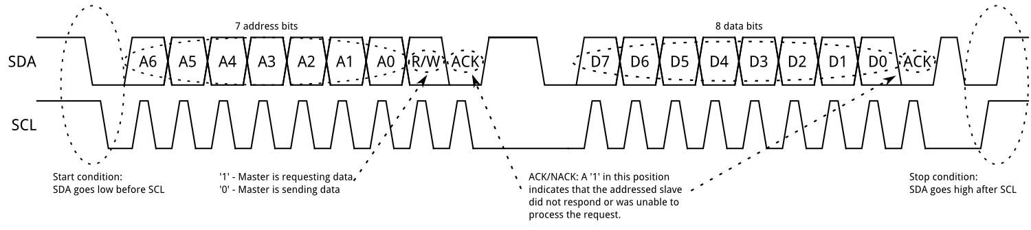