Reflow Oven: Software

Disclaimer: I am not a programmer, so you’ll have to forgive my bad habits and general inefficiency when it comes to programming.

Arduino code is composed of two parts: the setup, which runs once at the beginning, and the loop, which runs over and over again. The setup portion of the Arduino code is very simple, and is mostly setting up pins, interrupts and communications, as well as driving the outputs of the Arduino to a known state. Most of it is trivial, but I will show how I set up the interrupts since I had to do some research for it.

Setting up button (PCI) interrupts
Arduino Pro Mini Pinout from Sparkfun

The three buttons are attached to pins A1, A2 and A3. I didn’t want to constantly sample these buttons, so I wanted to use an interrupt to do that. As you can see in the pinout above, A1, A2 and A3 all have PCINT (Pin Change INTerrupt), which means the Arduino will interrupt the code when any of the buttons changes state. To enable the interrupts, you have to enable the interrupt (line 1) and then unmask the pins that can generate an interrupt (lines 2~4). You can read about the relevant registers for this interrupt here.

Setting up timer interrupt

I wanted to sample the thermocouple at a constant frequency. This cannot easily be achieved using polling, so I needed to set up an interrupt for that too. I decided 25 ms between samples was a good number; fast enough to monitor the data, but not too fast to the point of redundancy. In order to set the interrupt, I had to put the timer in the correct mode (line 3), put the 8 MHz clock through a 1024 divider (lines 4~6), set the threshold to 196 (line 7) and then enable the interrupt. As line 7 shows, 196 is the threshold I used because it gets me a value of about 40 Hz, which will generate an interrupt about every 25 ms. You can read about the relevant registers here.

Architecture in the loop

Within the loop, the architecture is as shown above. I’ll go into the ISR (Interrupt Service Routines) first.

An ISR is exactly what its name says; when an interrupt is triggered, a piece of code is executed to service that interrupt. An important characteristic of ISRs is that they need to be fast; since you’re interrupting a piece of code, you want it to be fast to minimize the impact you’re having on the rest of the system. Therefore, you shouldn’t have print statements or really long function calls. Fortunately, for this project, nothing is super timing critical.

PCINT ISR

As I mentioned earlier, I didn’t want to poll the buttons; however, I will poll the flag (buttons_flag) that is set when the buttons have changed states. In this ISR, I set the flag and then grab the state of the buttons. Because PINC is a register that has the state of all the pins on port C, and I only care about three of the pins, I mask the data from that register to only look at those three pins.

Timer ISR

When the timer interrupt goes off, it is time to get new temperature data from the thermocouple module. I first set the flag to indicate that new data is available, then perform SPI communication to the module to get the data. I put the retrieved data into an array (temp_array) after converting the data from bits to floating point. In order to make the data slightly more stable, I make oven_temp an average of 5 data points. ref_temp is the temperature of the thermocouople module itself (as in the IC), which I only keep track of for logging purposes. What we’re really after here is oven_temp, which is the temperature of the thermocouple located inside of the oven. As I stated earlier, an ISR should be fast, so I’ll move the SPI communication, floating point conversion, and averaging to outside the ISR. However, writing the code this way on the first draft helps me keep it straight in my head.

The UI state machine is the most complex part of the code. It determines what the push buttons do, what to display on the LCD screen, and what the temperature in the oven should be. The state machine starts off in the SELECT state.

Code when state machine is in SELECT state

When the machine is in the SELECT mode, it displays either “Profile” or “Manual” on the LCD; pressing the left or right buttons will change which of those two is displayed. Pressing the middle button will cause machine to change from SELECT to either PROFILE or MANUAL, depending on what was being displayed on the LCD. The code keeps track of start_time, which is important for calculations later on.

Code when state machine is in MANUAL state

In MANUAL state, the left and right buttons will allow you to adjust the temperature that is displayed on the LCD; pressing the middle button will cause the set temperature to update to the value shown on screen, causing the oven to heat up to that temperature. The temperature can be set from 30 to 300 degrees Celsius. Pressing left when at 30 degrees will show the text “Cancel”, and if you hit the middle mouse button at this point you will go back to the SELECT state.

Code when state machine is in PROFILE state

Here, the left and right buttons don’t do anything, and the middle mouse button allows you to abort the profile. Unlike in MANUAL state, where the set_temp was adjusted manually, in PROFILE state set_temp is calculated based on the inputted profile and the amount of time that has passed. The really long equation that determines the set_temp value is linear interpolation. For example, if the profile is 100 °C at 30 seconds and 200 °C at 90 seconds, then set_temp is 125 °C at 45 seconds, 150 °C at 60 seconds, and 175 °C at 75 seconds.

LCD update code

str1 and str2 are determined in the UI state machine. I initially had the LCD update on every iteration through the loop, but that caused the LCD to flicker very badly; evidently updating causes the screen to clear for an instant, so the constant updating meant constant flickering. Therefore, the LCD only updates if str1 and str2 are different from what was already on the screen. str1 is the first line of the LCD screen, while str2 is the second line (my LCD module is 2 lines of 16 characters, for a total of 32 characters available to display at once).

Turning relay on or off

Here is where the code actually turns the relay on or off. relay_enable is set by the UI state machine; in the SELECT state, the relay is not enabled. In MANUAL, the relay is enabled when the user updates set_temp, and disabled when the user goes back to SELECT state. In PROFILE state, relay is enabled at the beginning and disabled at the end of the profile. This prevents the relay from turning on (or remaining on) by accident. I also added hysteresis to make sure the relay doesn’t flicker on and off rapidly, since that would impact the life of the relay as well as cause current and voltage surges on the heating elements and the relay, which would be bad. For example, if set_temp is 70 °C, then the relay will remain on until the oven temperature exceeds 70 °C, at which point it will turn off. Then, the relay will turn on again when the oven temperature drops below 68 °C. Hysteresis puts (in this case) 2 degrees Celsius between the relay turning on and off.

This would also be the part of the code for implementing a more complex controller. For example, you could implement a PID (Proportional – Integral – Differential) controller here to get better settling time and reduce overshoot. For now, I’ll keep the relay control simple and see if I need a more complex one as I do testing.

Serial communication for debugging purposes

Lastly, I use serial communication for debugging purposes. As the Arduino runs, I can see what the oven temperature and set temperature is, and whether or not the relay is on. I can then make sure the code is operating as expected. Note that the serial communication occurs only when the relay is enabled; not much point in monitoring the state of the oven if the relay can’t be turned on. Note that relay enabled does not mean the relay is on; it just means the relay CAN be on.

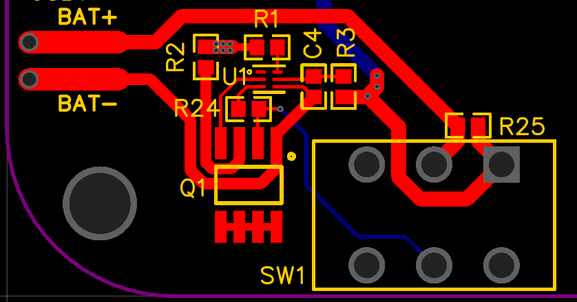
I’ve soldered the Relay Board, and the User Interface Board. Using both, I’ve done some benchtop testing. Now, I’ll have to integrate it into the oven and run a test to see how closely the oven can keep a constant temperature, and how well it can follow a profile.

Reflow Oven: Intro

For my next project, I’ve decided to build a reflow oven. It will be a very useful tool to have if I want to use components on my PCBs that have exposed pads or no leads, as well as make soldering much easier, faster and more consistent.

Toaster ovens are most often used for this project; they provide ample room and the heating elements provide the heat necessary for the solder to reflow. However, after looking around I decided to go with the Black + Decker TO2050S. It’s fairly cheap, has 4 heating elements as opposed to the usual 2, and has a fan built in that circulates the air, allowing for more even temperature across the PCB, which will prevent parts from getting too hot or cold. I bought my oven at Bed Bath & Beyond, but you can also find the unit on Amazon.

The project is relatively simple from an electronics point of view: you have an oven modified so that a microcontroller can turn the heating elements on or off, along with a thermocouple that the microcontroller continuously monitors. If the temperature in the oven gets too hot, turn the elements off; if too cold, turn it back on. The temperature that the microcontroller tries to set the oven varies over time and is set by the thermal profile you’re looking for, which will largely depend on the solder you’re using.

The microcontroller will control the heating elements using an electromechanical relay. A lot of projects I’ve looked at use a solid state relay, but I couldn’t find one that fit my vision for the project. My oven is a 1350 W unit at 120 V, which means it will draw 11.25 A. Most solid state relays I’ve found are rated for that much current, but they require heatsinks because the load causes the relay to get hotter over time. The heatsinks are substantially larger than the relay itself, and it adds to the cost of an already expensive relay. I’ve therefore decided to go with a traditional relay since it is cheaper and does not require a heatsink. One drawback that the electromechanical relay has is that it can only drive resistive loads; the fan in the oven is an inductive load, so I had to modify the wiring. The fan will be controlled by the timer dial of the oven, while the heating elements will be controlled by the timer and the relay in series. The timer, in addition to controlling the fan, will act as a fail-safe so that the oven cannot run longer than the set amount of time. This will protect the oven from running forever in case the microcontroller does something stupid.

I’ve decided to keep the microcontroller simple; I’ll be using an Arduino Pro Mini with 3.3 volt logic. The built-in bootloader, the simple nature of the algorithm and lack of need for specialized hardware make the Arduino fine for this application. The Arduino will be talking to a thermocouple (3.3V) module through SPI in order to read the temperature of the oven, and provide a user interface through an LCD (5V) and buttons.

Here’s a block diagram of the circuit:

Reflow oven FBD

Note that the relay is actually on the relay board, but the FBD does not reflect that for clarity.

I have to order most of the parts for this board (LDO, relay, thermocouple module, buttons), but I’ve started on the wiring:

Oven, before modifications
Oven, after modifications

You can see I removed 2 of the three dials, added a USB wall adaptor that’s been modified to output 5 volts over wires, and the two wires that are hanging near the bottom center of the oven connect to the relay. I’m thinking of putting the relay board above the USB adaptor, but I would have to see how big the board will be first. For the sake of safety, I’m trying to keep all the 120 V parts inside the oven. I’m planning on placing the User Interface Board where the two removed dials used to be. Also note that I’m using crimps and quick connect terminals instead of solder due to the high voltage and current in the system.

Once the parts come in, I can make the circuit and do a quick test to see how quickly the temperature can ramp up and what the maximum temperature the oven can get to is. There are a couple of ways to improve both these: adding insulation, adding more heating elements, or changing the wiring to draw more power. In addition, you can improve the solder quality by using a more complex control algorithm, where the top two and bottom two elements are controlled separately. I’ll have to see if these are necessary after achieving basic functionality.

Pocket Power Supply: Build + Test

Behold! My first finished project for this blog! The board works great, but there are definitely some changes I would like to implement if I ever do a respin of the board. The enclosure also came out a lot more… homebrew than I had in mind, but it works, so it’s fine with me!

Assembly

Getting the power supply built took a couple of hours. Here’s the picture of the finished product:

One thing I vastly underestimated was soldering chips with exposed pads. The videos on YouTube made it look so easy! This was doubly true for the buck boost regulator, U4, near the right on the picture above, right below the inductor. U5 and U1, near the top left and bottom left respectively, also were difficult to solder. U5 also has an exposed pad, while both U1 and U5 are leadless chips. I was able to solder U4 on with the help from a friend (he had a board pre-heater and a hot air blower), and I was able to solder U4 and U5 to the board myself. However, I’m not sure if I was able to fully solder U5’s exposed pad; however, I did make enough of a connection to make the board work. U5 is a linear regulator, so it can get very hot, making the exposed pad connection crucial for maximum performance. However, due to the lack of proper tools, I may have to live with a reduced maximum current input and output for this chip. Fortunately, the chip has a thermal limiter built in, so the chip should stop itself from self-destructing.

One piece of advice that applies to all board assemblies: solder the big components on last. The two big connectors on the left and right end of the board, as well as the switch near the bottom make reworking the board a pain in the butt; they always get in the way of your solder or iron. It makes testing as you build a pain, but it’s definitely worth it.

The enclosure is an Altoids can that I dremeled to fit the board. The board was designed to fit inside the can, but the connectors, potentiometer and switch had to have cut outs so that the lid could close with the board inside. a hole was also drilled for the LEDs to be visible, which indicate the status of the battery when it’s being charged. Lastly, the bottom of the can had holes for the stand-off screws. There were a lot of burrs and sharp edges when I finished cutting the metal (which is very thin) with the carbon discs, so I used the sander attachment for the dremel as well as a small file to smooth everything out. Lastly, I used a wire well to make the metal edges easy on the fingers. Works well enough, but again it looks very homebrewed, which I’m personally fine with.

The LiPo battery is sandwiched between the PCB and the bottom of the tin. The battery itself is taped to the bottom of the board to prevent it from shifting around.

Testing

  1. To test the BMS (U1), I hooked up the battery pads to an adjustable power supply, and powerd the board through fly-leads. When the power supply was at 3.7 V, the battery charger tried to force current into the power supply, since at that voltage the power supply looked like a partially depleted battery. WHen I raised the power supply to 4.2 volts, the blue led (which indicates the battery is being charged) turned off, indicating the BMS correctly cut off current when the battery was charged enough. When the power supply was adjusted back to 3.7 volts, the blue LED came back on. To test the undervoltage detection of the BMS, I disconnected the fly-leads and set the power supply to 3.7 volts, and measured 3.7 volts on BAT+ test point with respect to GND. I started to drop the power supply voltage, and the voltage at BAT+ changed as well. When the output voltage became 2.8 V, the voltage at BAT+ dropped to 0 volts, indicating the BMS disconnected the battery from GND. To check the discharge overcurrent circuit, I hooked up various loads to the output of the circuit. When the battery is at 4.1 volts and the load is 400 mA, the voltage at GND with respect to BAT- was 0.0327 volts. Since the cut-off is 0.1 volts, you can extrapolate this to see that that the cut off current is 1.2 A. The battery I was using is rated for that output, so this works for me. I did testing at different loads, and got the same results. However, I noticed that as the battery voltage got lower, the current limit decreased; when the battery is at 3 volts, the current limit is about 0.5 A.
  2. To test the battery charger (U2), I hooked up the circuit the fly-lead connectors to a power supply set to 8 volts. The switch was set to connect the battery to the circuit. When the power supply output was enabled, the circuit drew 100 mA, which meant that the battery charger was charging the battery with the correct amount of current. When I changed the programming resistor from 10 kΩ to 2.2 kΩ, the circuit drew 450 mA. Again this was the expected result. The testing of the BMS earlier showed that the battery charger knew when to stop charging.
  3. To test the UVLO feature, I put 5 volts across the fly-leads, which drew no current. When the voltage was set above 7 volts, the circuit drew current. This indicates that the UVLO operates as expected.
  4. The linear regulator (U5) was tested by inputting 7 to 12 volts through the fly-leads, and the output was a constant 5 volts. The regulator was successfully able to maintain this voltage even when the battery charging circuit drew 450 mA, though this made the linear regulator very hot.
  5. When the circuit is powered through USB, the circuit drew around 450 mA when the battery was charging. When the circuit is powered by 7.3 volts and USB, it draws 0 mA through USB and 450 mA through the 7.3 volts, which indicates that the power multiplexing design works as expected.
  6. When the battery is connected to the circuit and 7.3 volts are provided through fly-leads, VDD is 7.3 volts with respect to GND. This indicates that the buck-boost circuit is not powered by the batteries, indicating the second power multiplexer also works as designed.
  7. The buck-boost circuit can output 1.2 volts when the potentiometer is set all the way to one side, and 13 volts when it is set to the other, which is expected.
  8. I tested the buck-boost circuit powered by battery only first. I found that when the battery is fully charged, the buck-boost regulator can output 8V at 456 mA, or 13 V at 280 mA. This means the circuit can output about 3.5 watts when the battery is fully charged.
  9. When provided external power, the circuit can output an impressive amount of power. I’ve tested 5 W, 10 W and 20 W outputs at various input and output voltages, and the results look pretty good. Note that low input voltage and high output voltage leads to large amounts of current, which can damage the UVLO and power multiplexing circuit.
  10. The output of the buck-boost was as noisy as I expected. The noise at light and heavy loads is less than 100 mV peak to peak, which is acceptable for my purposes as I plan to use it to power digital circuits with 3.3 or 5 volt logic, or circuits that don’t care about noise such as small fans or motors. If you want to use this for an analog circuit or a noise sensitive application, put a filter on the circuit you’re powering. I didn’t put a filter in this design because (a) not every application needs a filter and (b) a filter would work better near the load rather than the power supply.

All in all, I’m very happy with the circuit. The UVLO, linear regulator, battery charger, BMS and buck-boost regulator do a fine job. The output power of the circuit, both on batteries and with an external power supply, far exceeded my expectation. All in all, I’d say the project was a success! Additionally, it’s nice that the enclosure works well since I really can carry an adjustable power supply in my pocket.

Future Design Changes

For those who want to modify my design, or if I do another spin of this board, then here’s a couple of pointers on what to change:

  • The BMS has a “handy” feature where the battery has to be “primed.” If the battery is disconnected from the circuit (through the switch or by cutting a wire), then the battery cannot be used again when it is reconnected to the circuit UNLESS you start charging it. You only have to charge the battery to start using it the first time after you connect the battery; however, if you have a habit of disconnecting the battery when you’re not using it, then it’s a pain in the butt to constantly hook it up to a charger. To solve this, it would make sense to put a bush button that can momentarily connect BAT- and GND. When the battery is reconnected, pushing the button will make the battery look like it is being charged, and the BMS will connect the battery back to the rest of the circuit. No charger necessary.
  • The UVLO is not as efficient as I had hoped. If the input voltage is 7 volts, then the gate voltage is about 6.2 volts. This means that VGS = -0.8 volts, which is not very much. Since VGS is relatively small, Q3 has a relatively large resistance; I measured 0.5 ohms at one point. When you’re trying to pump an amp through Q3, a resistance that large can cause problems, as VIN will be noticeably smaller than VIN_RAW. I suggest changing the UVLO so that when VIN_RAW is above a certain point, something yanks the gate of Q3 down to GND, which will greatly improve efficiency. Additionally, I would recommend changing Q3 to a bulkier transistor if you want to output serious amount of power; the transistor is only rated to 1.4 A, which will throttle your maximum output power.
  • I could of sworn I saw the RUN pin tied to VCC in the datasheet. Unfortunately, this does not work; VCC does not output a voltage, which keeps the RUN pin low, which prevents VCC from outputting. I changed the circuit so that RUN is pulled up to VDD instead of VCC; this fixes the problem. You can actually see that rework in the photo of the board (orange wire).
  • For some reason when I was designing the board, I was only thinking of USB ports on laptops and computer towers, which can only output small amounts of current. If I had realized that I could just use a wall wart to get a 1 A or 2 A capable USB power source, then I think it would have made more sense to charge the battery solely through USB and not at all through VIN. While charging the circuit through VIN is convenient because it lets you charge the battery and power the buck-boost regulator, it puts a lot of restrictions on VIN. (1) As VIN voltage increases, the linear regulator generates more and more heat, which shortens the chips life span and risks triggering the thermal limiter, which will cause the battery charging circuit to be sporadic. This is especially problematic at high battery charging currents. (2) Q3, the pass transistor in the UVLO circuit, is rated for 1.4 A, which means that at 450 mA battery charging current, you’ve used up about 33% of the current budget for the battery alone. Removing the linear regulator would also make board assembly easier since that’s one less component with an exposed pad and leadless package.
  • I was hoping I could use R2 to adjust the current limit on the BMS; since BMS looks for GND to be within 0.1 volts of BAT-, I thought adding a resistance in series with the transistors would allow me to adjust what the voltage differential was for a given current flow through the battery. Alas, this is not the case; the circuit is more complicated than that, so R2 should just be left as a 0 ohm. I would like to look into how to properly adjust he current limit, but for now since the BMS happens to limit the current to values that work for me, I’ll put that on a future list of things to look into.

Despite the quirks and things to keep in mind, I am very happy with this project. I hope you enjoyed reading about the project’s development! For my next project I’m thinking of converting a toaster oven into a solder reflow oven. I guess I was pretty traumatized by trying to solder exposed pads using a soldering iron…

DESIGN FILES

OpAmp: Basics

The operational amplifier, usually referred to as an opamp, is a very useful component in the world of electronics. It has at least 3 ports: a non-inverting input (marked with a +), an inverting input (marked with a -) and an output. It also has 2 power rails, which (roughly) define the highest and lowest voltages it can output and receive. The opamp allows designers to manipulate signals in the following ways:

  • Amplify or attenuate the signal
  • Increase or decrease offset
  • Turn differential to single-ended, or vice-versa
  • Combine multiple signals into one
  • Act as a buffer
  • Convert current to voltage, or vice-versa
  • Filtering
  • Multiple of the above

The opamp, in short, allows designers to implement mathematical operations and much more, hence the name. I’ll get into examples in another post, but first, how does it work?

The operational amplifier, in isolation, is very simple. It takes in two signals and outputs the difference between those two voltages times a very large number in other words:

A, the gain of the opamp, is “very large” which can be anywhere around a thousand to tens of millions. This by itself isn’t very impressive; if you have an opamp with a gain of a thousand, then you can turn a signal that’s a couple of millivolts into one that’s a couple of volts. But even for this simple application, the opamp struggles; the gain is not very well characterized, tends to change with temperature and time, and varies between chips. In other words, opamps generally are not meant to operate in this mode. However, one application for this is as an analog comparator; if VIN2 > VIN1, then the opamp will output the highest voltage it can, and if VIN2 < VIN1, then the opamp will output the lowest voltage it can. If the opamp is powered by 0 volts on its negative rail, and 3.3 or 5 volts on its positive rail, its output could be interpreted as a logic low or logic high. However, there are analog comparator ICs that do this function much better, so again this is not the ideal application of opamps.

The opamp becomes a very powerful tool when it has negative feedback, or when the output of the opamp has a path back to the negative input. When an opamp has negative feedback, it has the useful property of forcing both its inputs to be the same value, which we’ll show below. Here’s the simplest opamp circuit with feedback:

There are 3 ways to understand how opamps work, in order of increasing complexity and accuracy:

  1. Intuitive: forget the equation I mentioned above, and think about the analog comparator example. The simplest way of thinking of an opamp is this: if the non-inverting input is greater than the inverting input, then the output increases. If the inverting input is greater, than the output decreases. If they’re the same, then the output stop changing. Using these three rules, let’s look at the example above:
    1. VIN and VOUT are both initially 0 V. Since both inputs are 0 V, the output does not change.VIN suddenly increases to 1 V, but VOUT is still at 0 V. Since the non-inverting input is larger than the inverting input, the output will begin to increase.When VOUT is at 0.5 V, the non-inverting input will still to larger, so the output will continue to increase. In this example, as long as VOUT is smaller than VIN, the output will continue to increase. In other words, as long as the non-inverting input is greater than the inverting input, the output will continue to increase.When VOUT finally reaches 1 V, both inputs will be the same, so the output will stop changing, VOUT will therefore have a final value of 1 V, which is the same as VIN. In other words, when both inputs are the same, the output stops changing.If VOUT overshoots by accident, say VOUT is 1.1 V, then the inverting input is now greater than the non-inverting input. In this example, as long as VOUT is greater than VIN, it will continue to decrease. In other words, as long as the inverting input is greater than the non-inverting input, the output will continue to decrease.
  2. Electrical Engineering: in school, especially in the electrical engineering undergrad, you’re told to assume that both inputs to the opamp are equal if you have negative feedback. This assumption allows you to derive equations quickly and easily:

3. Control Systems: below is a simple model of the opamp shown previously

Here, E is the error signal (difference between the non-inverting input and inverting input), A is the gain of the opamp, and VOUT = A / (1+A) * VIN. In the Intuitive and Electrical Engineering method, we got VOUT = VIN. However, the Control Systems method shows that the output actually depends on the gain of the opamp. As mentioned before, the gain A is very large, and the larger A is, the closer VOUT and VIN are; at A = 1000, VOUT is 99.9% of VIN. This is the reason the gain A does not need to be very well controlled for most applications; as long as it is “very large,” you can assume the opamp is working correctly (ie. the assumption that both inputs are the same holds). However, as we’ll talk about in a future post, A varies with frequency. As the frequency of the input increases, A starts to decrease. Eventually, A will be small enough that the assumption VOUT = VIN no longer holds. For example, when A = 5, VOUT is only 83% of VIN; at A = 1, VOUT is only 50%.

The control systems approach will give you the most information about the opamp. It’ll tell the designer about the error on the output, transient response and stability. But for most purposes, the electrical engineering approach is sufficient; assuming both inputs are the same voltage will allow you to very rapidly and accurately analyze how circuits behave; for this reason we’ll be using it unless there’s a reason not to. Here area a couple more examples of what opamps can do:

Non-inverting gain
Inverting Gain
Voltage Subtractor with Gain
Voltage Adder

Pocket Power Supply: Layout

After completing the schematic last time, here’s the layout! I’ll give a quick overview, and then go into the layout of each piece:

  1. Input power from fly-leads and UVLO
  2. Linear regulator and mux for battery and fly-lead power
  3. USB power and battery charging circuit
  4. Battery power, BMS and switch
  5. Pads for GND and VDD, 100 mil spacing
  6. Buck-boost circuit, output connector

Note that in the picture above, as well as other pictures of the layout, the ground pour has been removed for clarity. Also the picture above only shows the top layer of this 4 layer board.

The top layer is for components and the majority of the traces. The second layer is a solid ground plane with no interruptions or sections cut away. The third layer is a power plane; the left half is for VDD, while the right half is split between VDD and VOUT. The bottom layer is for miscellaneous routing. Note the test points near the top left and bottom right of the board. These will be used to test the board during the assembly process.

Fly-Lead Power, UVLO, LDO, Mux

J1 is where the fly-leads will provide power to the board. C19 is a bypass capacitor providing local power; this will allow the fly-leads to only carry low-frequency and mostly DC current, while the higher-frequency and transient currents will be kept local to the board. The traces coming out of J1 were made as thick as possible to minimize losses, as well as maximize amperage. However, the thicknesses were limited by the size of the pads, primarily Q3. Coming out of Q3, the fly-lead power goes to two places. First, the fly-lead power feeds U5, which is an LDO. The LDO regulates the fly-lead power down to 5 volts and outputs to the cathode of D2; in the event J1 has no power, USB power, which will be on the anode of D2, will power the battery charging circuit. Fly-lead power also carries on to D1’s anode, providing a potential source of power to the buck-boost converter.

The only thing to point out here is, besides the general good practice of having bypass capacitors close to the chip they are bypassing (C3, C18 and C2 are bypassing U5 in this case), U5, the LDO, uses the PCB itself as a heatsink since it dissipates a large amount of heat. To keep the chip cool, the ground pour on the top layer connects to the exposed pad, and the vias in the exposed pad connect directly to the GND plane. Both of these large copper planes will act as heatsinks.

Left: Top side, Right: Bottom side

In order to solder the exposed pad of the chip to the PCB, a hot air blower is required since the entire chip needs to be heated up. I tried a couple of things to get around this requirement: I exposed copper on the top side as well as on the bottom. The top exposed copper connects directly to the ground pour and is right next to the exposed pad. If a soldering iron is placed on this pad, then it should be able to heat up the exposed pad enough to melt solder, thus fusing the chip to the board. I was worried that since the exposed copper also connects directly to the ground pour, it may have a hard time heating up the exposed pad. I therefore also tried putting exposed copper on the bottom side of the board. On the bottom side, the exposed copper does not directly touch the ground pour on the bottom, so heating up the exposed pad should be easier. It does, however, go through vias and connects to the ground plane, so we’ll have to see which method works better.

USB, Charging Circuit

Similar to C19 above, C20 provides bypassing to the USB power; any transient current requirements on the board will be fulfilled by C20 rather than through the USB power supply. As mentioned above, D2 provide power multiplexing; if no power is supplied through J1, then D2 will allow the USB to power the battery charging IC, U2. U2 is bypassed by C1 and C5, and uses R4 and R5 for temperature sensing and current limiting, respectively. R6, R7 and R8 provide current limiting for D3, D5 and D6, which are LEDs, so their layout is not critical. Note that C1 bypasses the output of D2, so it provides bypassing for U2’s input, while C5 provides bypassing for the output, which connects to the battery pack (after the switch).

Battery, BMS, Switch

BAT+ and BAT- indicate where the battery wires should be soldered to. This board was designed for the battery to go onto the bottom side, so the pads are through hole. In case someone wanted to try feeding wires from elsewhere, or wanted more pad to solder to, I extended the pad into a rounded rectangle. From BAT+, the trace goes to the switch, with R25 providing a way around the switch if the need arises (battery can only support 500 mA), while BAT- goes to the dual transistor pack, Q1. U1, the BMS chip, turns Q1 on and off, connecting or disconnecting the battery’s return current. C4 provides bypassing to U1, so they’re close together. Lastly, the traces going to R2 from Q1 and R3 from SW1 are made as thick as possible to provide the least resistance, since the battery will be the majority of its current through these traces during operation.

VDD and GND Pads

While laying out the board, the dimensions of which are made to fit inside an Altoids can, I realized I had way more room than I needed. I decided to fill the empty space between the power conditioning circuitry and the buck-boost regulator with a bunch of VDD and GND pads. The primary reason was I did this was so that the board could be cut in half. In applications where you just need power conditioning, or you just want the buck-boost regulator, you can cut the board in two and just use half of it. The pads will a place to get the conditioned power, or provide power for the buck-boost regulator. I also made the pitch 100 mils to comfortably fit regular pin headers. Lastly, the plated through holes and vias provide thermal conductivity from the top to the bottom of the board, as well as to the planes in-between, so if one part of the board heats up, then there is a thermal path to the rest of the board.

Buck-Boost Regulator

The buck-boost regulator has the most sensitive layout, since it has high-frequency switching. To minimize losses as well as minimize inductance, several pads have been combined together into one large copper trace. This was done for the traces going to the inductor, near the top of the image, as well as the power input to the regulator near C13. In addition, to minimize inductance on the output, C8, C16 and C14 have the fatest possible traces, as well as many vias connecting them to the ground and power planes. The multiple vias will minimize inductance and resistance between the capacitors and the planes, which will help reduce noise. Similarly, C17 and C13 have multiple vias; however, due to layout, I could not place those two right next to each other. However, because they connect through multiple vias to power planes, and since C17 is a bulk capacitor, the suboptimal placement of C17 should be acceptable.

Small section on left is VDD, rest if VOUT

Pocket Power Supply: Schematic

Before going into the details, I’ll talk about how the high level design has evolved:

  • There are 3 potential sources of power: the fly-leads, the USB and the battery. I’ve decided that the USB should only charge the battery, and not power the output regulator directly. This was done to 1) reduce the complexity of the power multiplexing and 2) limit the current draw through the USB. Limiting the current draw on the USB is very important as trying to draw too much may damage the USB port on the power source side; for example, if it’s plugged into a laptop, the laptop may be damaged. Conveniently, the battery charging circuit will have a current limit to protect the battery; in this case, it will double to protect the USB as well.
  • The fly-leads are assumed to be capable of outputting a large amount of current over a wide range of voltages; say up to 12 volts. Because of this, the fly-leads will be given priority over USB when it comes to charging the battery, and it will be chosen over battery when it comes to powering the output regulator. This way, you can provide power through fly-leads and not load the USB port or the battery.
  • There will be 2 power multiplexers. The first will choose between the fly-lead power source and USB for charging the battery; this will be done by comparing the two sources and going with the one with higher voltage, accomplished using a diode. The second will be choosing the battery voltage or the fly-lead to power the output regulator. This will be done by checking if the fly-lead power is present, and choosing that if possible. In both cases, if the fly-lead power is close in voltage to the USB voltage or the battery voltage, the multiplexer may become confused or current may flow in the wrong direction. To prevent this, the fly-lead power source will have an UVLO (under-voltage lockout) circuit, which will prevent the fly-lead power source from providing any power until the voltage exceeds a certain amount.
  • The wide voltage range that the fly-leads could be presents a problem for the battery-charging circuit for two reasons. One, the battery charging IC can only accept voltages up to 6 volts. Two, even if it could accept 12 volts, it would output at worst case around 3 volts. This means that it would have 9 volts across it, and since most battery charging ICs are linear (as opposed to switching), this will mean the chip will have to withstand a large amount of heat dissipation. This concern was addressed by putting a linear regulator on the input of the battery charging circuit.
  • I’ve added a switch to disconnect the battery from the circuit. When not in use, the circuit’s power consumption is low, and the BMS (battery management system) IC should prevent the battery form being drained too much. However, for long term storage (or to make sure the battery is not loaded), the switch will completely disconnect the battery from the circuit, preserving energy.
  • The circuit is designed to use a lithium-ion / lithium-polymer battery that can tolerate a voltage of 2.75 volts to 4.232 volts. The maximum charge and discharge rates can be adjusted, but for now are set to around 100 mA.

The updated functional block diagram looks like this:

Updated Functional Block Diagram

Here’s a breakdown of the schematic:

Fly-lead input + UVLO

The fly-leads will come onto the board on J1. I wanted the project to be as user-friendly as possible, so J1 was selected to be a connector that didn’t require tools to insert and remove wires.

The UVLO circuit works by using 2 components: a PMOS and a zener diode.

  • A zener diode is like a regular diode except it has a very low breakdown voltage. This means that the zener diode will not conduct current until the voltage across it exceeds a certain amount (around 7 volts in this case); then, the diode will try to resist a further increase in voltage by conducting current. The diode can begin to conduct a very large amount of current, so it is current limited by the 100k resistor.
  • The PMOS will not conduct current until the gate is certain number of volts below the source. The source connects to VIN_RAW, while the gate connects to the cathode of the zener diode.

The circuit operates as follows: when the input voltage is below 7 volts, the zener diode does not conduct current. Thus, because there is no current drop across the 100k resistor, the source and the gate of the PMOS are the same, meaning the transistor does not conduct. When the input voltage exceeds 7 volts, the diode will conduct, forcing the gate to remain around 7 volts, while the source will exceed 7 volts. Since the source now has a higher voltage than the gate, the PMOS will conduct, allowing the rest of the circuit to be powered by the fly-leads.

The PMOS allows the power source to be disconnected from the circuit by cutting off the high voltage. However, another way to kill power is disconnecting the ground connection. Disconnecting the ground is preferred in most cases, as to disconnect the ground, an NMOS is used, which is more power efficient than a PMOS. However, I opted to use a PMOS in case the USB and the fly-leads shared the same ground. If they did in fact share the same ground, and an NMOS was used, than the UVLO circuit would not work.

Linear Regulator and USB

The fly-lead power supply then goes into a linear regulator, reducing the voltage to 5 volts. I initially wanted to use a regular linear regulator; however, the drop-out voltage requirements (which sets the minimum usable input voltage), made using a regular linear regulator an unattractive option as it would reduce the functional voltage range for the fly-leads. I therefore decided to use an LDO (low drop-out) regulator. I was wary of these devices because their stability often depends on the ESR (equivalent series resistance) of the output capacitor, which sounds very shady to me. That’s right: if you use a ceramic capacitor (which has minuscule ESR in most cases), the regulator will not work! However, I found the NCP3337, which has many attractive features like being stable with any type of output capacitor, no need for external compensation, simple input and output bypass capacitor requirements, and reverse current protection. The last feature is very useful in this case, and is the reason why the output of the regulator doesn’t require a diode to protect the power supply connected to the fly-leads.

The USB connection is very simple. The connector will provide a connection to a micro-USB cable, and the diode will prevent the linear regulator from driving current out onto the cable. The diode is a low power Schottky diode, which has a relatively low forward voltage drop. The low forward voltage drop will improve power efficiency of the system.

Battery Charger

The battery charging circuit has the MCP73833 at its heart. The battery charger will output a constant current when the battery is not almost full. This current value can be set by changing the resistor value connected to the PROG pin (10k in this case, setting the current to 100 mA). When the battery is almost full, the charger will change to a constant voltage mode, which will cause the battery to charge more slowly. What the output voltage is depends on the chip’s part number. For this design, we assume the battery should not be charged above ~4.2 volts, so I got the chip that will only output a maximum voltage of 4.232 volts. The LEDs will show the status of the input voltage and the battery charging, which is very useful, but can be removed if not needed. Lastly, a thermistor can be used in this circuit, but is not used in this application.

BMS

BQ297000DSER is the BMS IC. It will disconnect the battery from the rest of the circuit if it detects that the battery voltage becomes too high or too low, or it detects the input or output current is too high. This will extend the life of the lithium-ion / lithium-polymer battery, but more importantly it will prevent the battery from exploding or catching fire. The IC monitors the overvoltage, undervoltage, overcurrent charge and overcurrent discharge conditions by monitoring the voltage on its V- pin and BAT pin.

The BAT pin sensing is pretty self-explanatory: if the battery voltage becomes too high, prevent charging; if the battery voltage becomes too low, then prevent discharging. Both of these actions are done by turning off either Q1.1 or Q1.2. V- sensing, on the other hand, I wasn’t as sure about; it’s attempting to measure current by measuring a voltage at one point. I suspect that the chip relies on the on-resistance of the NMOS transistors (Q1.1 and Q1.2) to generate a voltage that is proportional (or close to proportional) to the battery’s output current. However, the on-resistance of the transistors is not a closely controlled value, and varies with the chip itself, time, temperature, etc. In addition, if you want to set a specific current limit, you would have to pick specific transistors that have a very specific on resistance. In order to ease this limitation, I put R2 in series with the transistors so that the on-resistance could be artificially increased, allowing the user to adjust the current limit by changing the value of the resistor. I also put a resistor in between the gate of Q1.2 and the output of the IC to prevent output contention, which I’ll talk about more in the next section.

As a minor note, I really don’t like this chips footprint because it it tiny and leadless, making it very difficult to solder. It also tolerates too much overvoltage for my liking. However, it was the best one I could find that was available and close to what I needed. The overvoltage shouldn’t be a problem as long as the battery is charged using the charging circuit discussed earlier.

Battery Switch

To quickly disconnect the battery for storage or to turn off the circuit, a switch was added to disconnect the battery from the circuit. SW1.1 will have current going right through it, so flipping this switch will disconnect the battery. The switch is rated for 500 mA, which is more than enough for this application. However, in case some want to have more than 500 mA, a 0 ohm bypass resistor can be added, saving the switch. But if you add that, how do you prevent the battery from discharging? That’s where SW1.2 comes in. During regular operation, SHDN is driven by the BMS IC, allowing it to turn on and off the discharge transistor as it sees fit. However, if SW1.2 is changed to the other position, SHDN becomes grounded, forcing the discharge transistor to turn off, electrically disconnecting the battery from the circuit. The 1 kohm resistor on the output of the BMS IC prevents the switch from shorting the output to ground.

Power Multiplexer

The power multiplexer chooses what will power the output regulator: the fly-lead power supply, or the battery. It does this by using a PMOS, and is somewhat similar to the UVLO circuit described earlier. If no voltage is supplied through the fly-lead connector, than the gate of Q2 will be near 0 volts, while the source will be close to the battery voltage. This will turn the PMOS on, and the battery can provide power to the output regulator. If voltage is non-zero at VIN (and thanks to the UVLO we know that the voltage will be 7 volts or greater in this case), than the gate voltage will be higher than the battery voltage (which goes up to 4.2 volts at most), so the transistor will remain off. This will prevent the battery from powering the output regulator. The transistor is the main reason the UVLO is necessary; if there was no UVLO, and VIN was about the same voltage as BAT+, than the transistor will be partially conductive, which will allow an unrestricted amount of current to flow from VIN to BAT+, which may damage the battery. The BMS should protect the battery at worst case, but I wanted to add an extra layer of security. The Schottky diode D1 prevents current from flowing out of the battery and going out through the fly-leads.

Buck-Boost Regulator

I chose the LTC3112 buck-boost regulator for several reasons, despite its high cost:

  • It has a very wide input and output voltage range
  • It has high output current capabilities
  • It has a model in LTSPICE, allowing the design to be tested

The circuit shown above is mostly similar to the one given in the datasheet. The only comment I have to make here is the feedback pin; I used a potentiometer to make the output voltage adjustable. R23 is a 1 megaohm potentiometer, and R13 and R14 are used to set the minimum and maximum output voltage of the regulator, which are (in theory) 1.24 volts and 12.47 volts. Another reason these particular values were chosen was due to the regulator’s requirement that the output impedance of the feedback path to the feedback pin must be greater than 100 kohms, which this design accomplishes.

I wish I could comment on the compensation network, which will define how the regulator reacts to transients and during start-up. However, this is a subject I don’t understand very well myself; I’m hoping to have a post about it at a later time exploring this subject. For now, I kept tweeking the values in LTSPICE and running simulations until I got a start-up behavior I liked. I’ll need to do testing after the circuit is built to verify the results, but for now I’ll use these values.

This is the same type of connector as the input connector for the fly-lead: no tools required. I also wanted to have more available on the connector than just ground and power output to make the design more flexible and user-friendly. I therefore added an enable pin, in case an external circuit wants to control the regulator, and IOUT, which indicates how much average current the regulator is outputting.

The resistor shown here set how the regulator behaves. SYNC can be tied high or low to make the regulator operate in PWM or Burst Mode respectively (latter is better suited for low power applications than the latter). OVP can be used to set over-voltage protection, preventing the regulator from outputting if the input voltage is too high. SYNC will be set to PWM, and OVP will not be used.

Conclusion

This concludes the overview of the schematic. We have discussed how the fly-lead power supply input will be conditioned, how the battery will be charged, how the battery will be ensured to operate safely, how the output regulator will be powered, and how it has been designed. Next, we’ll move on to the layout, where I do an overview of the layout.

Pocket Power Supply: Intro

The first project that I’ve decided to work on for this blog is a power supply project. I’ve designed a power supply before, but it was way too bulky. My first one was more along the lines of a bench-top power supply; it took in 120 VAC, had multiple outputs, one of which was adjustable, and could output 500 mA on each output. However, I’ve come to realize that such a power supply may be difficult for those with small tables, which is my situation. I also realized that the power supply is extremely heavy and a pain to carry around. Both of these were due to the power transformer inside the power supply. I wanted it to be a linear power supply, which requires very, very large and heavy transformers.

So for this power supply, I wanted something slicker and portable. My goal is to get a power supply that fits inside of an Altoids can; therefore, it will take up small space on your desk, easy to store, and event portable if you put a battery inside of it. The specs are as follows:

  1. The project shall be safe to the user as well as the devices powering it.
  2. Power supply shall fit inside of an Altoids can, or something very similar.
  3. Power supply shall have one, adjustable output.
  4. Power supply shall work without an external power source.
  5. Power supply shall provide option of powering over USB.
  6. Power supply shall provide option of powering through fly-leads.

The design goals are as follows:

  1. Project is user-friendly; easy to use, easy to modify, and provide documentation.
  2. The output range should be large. Something in the ball-park of 1 V to 10 V.
  3. The output current is not expected to be large when powered by USB or the LiPo battery; this project is meant to power simple digital circuits, not motors or power LEDs or anything like that.
  4. The output current capability should be significantly larger when the fly-leads are used, since they can be used to provide much more input current.

There are 2 main sources of complexity in this project. Spec #4 states the device will work without any source of external power. This means the project must have some sort of battery. I think the best option would be a lithium-polymer battery. LiPo batteries are rechargeable, have high energy density. Lithium ion is basically the same, but I feel LiPo would fit better within an Altoids can. Disposable batteries may also work, but ultimately recharageable is more convenient and portable than disposable batteries. Also I’ve never used LiPo batteries before, so it’ll be a fun experience.

The second source of complexity is the multiple sources of power; specs #5 and #6. There are two portions of the project that will need power: the battery charging circuit, and the output regulator. The battery charging circuit will have to choose between the USB and the fly-lead power supply. It will have to make sure no conflict occurs when both sources are providing power, and be able to charge the battery no matter what kinds of combination the input power is (both, one or the other). The output regulator, which will condition the output of the circuit to what the user needs, has an even more complex task. The output regulator has the following potential sources of power: USB, fly-leads, and the battery itself. The output regulator circuit must account for all possible combinations of power sources.

The battery charging circuit is pretty straight forward from a high-level overview: the circuit will choose either the USB or the fly-leads as a power source, and feed it to a battery charging chip. There are several safety precautions that must be addressed, but we can dig into those later. But what will the output regulator look like?

The output regulator will need to be designed without assuming a set input voltage. This is because the fly-leads can provide almost any voltage (within reason), and the battery voltage changes as the battery is charged or discharged. As such, the requested output voltage may be above or below the input voltage; for example, a typical LiPo battery has a voltage range of 2.8 V to 4.2 V, but the desired output may be 3.3 V. The output regulator should therefore be a buck-boost regulator or a SEPIC (single-ended primary-inductor converter), both of which can produces output greater than, less than or equal to the input voltage. I decided to go with a buck-boost regulator topology since it is more power efficient. A SEPIC topology has the advantage of a simpler, and therefore cheaper, power regulator IC, but the fact it needs two power inductors as opposed to buck-boost regulator’s one means it will need more board space, as well as suffer from power inefficiency due to loss in the inductors. I’m planning on elaborating on the details in a future post.

Here’s a rough first draft of the design I have in mind:

Functional Block Diagram

Full confession: I’ve been working on this project a while before I started the blog, so I know the design has changed quite a bit from the FBD shown above, but I wanted to show the sketch I had made when I first started this project. Next, I’ll discuss the schematic (probably in 2 parts), then the layout, then how the circuit behaves after I build + test it.

Design a site like this with WordPress.com
Get started